Simulation and modeling play key roles in high-power diode-laser packaging
JINGWEI WANG, TUANWEI FU, and XUEJIE LIANG
High-power diode-lasers (HPDLs) are now widely used for industrial (materials processing procedures such as welding, cutting, surface treatment, etc.), scientific, and medical applications. The need to design advanced high-power laser packages, to understand the physics of the behaviors of these packages and its interfaces, and to prevent possible functional (optical) and mechanical (physical) failures are of obvious practical importance. As laser technologies develop, the output power of HPDLs has grown, along with the cavity length of diode laser bars increasing from 1 to 4 mm. As a result, the waste-heat energy density of a single diode laser bar has increased dramatically from 200 W/cm2 to more than 600 W/cm2.
Many failures in HPDLs—for example, bonding interfaces—are directly related to the packaging.1 Thermal behaviors of the bonding interfaces and thermal stresses between the bonding interfaces are the major factors affecting the functional and structural performance of HPDLs. If the accumulated heat cannot readily escape, the elevated temperature and thermally induced stress at the location of the p-n junction will not only adversely affect the output power, slope efficiency, threshold current, and device lifetime, but could also cause spectral broadening and wavelength shifts.2 The emitting wavelengths will shift if the junction temperature of the emitters across the array is not well controlled and/or not uniform. The above-mentioned scenarios make the thermal management of high-power laser devices a major challenge in designing, manufacturing, and utilizing HPDLs.
Simulation and modeling of thermal stress in packaging of HPDLs
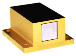
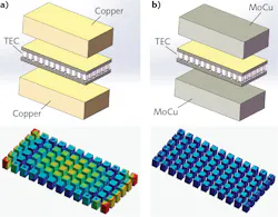
During the design process, the coefficient of thermal expansion (CTE)-matched principle was taken into account as a crucial factor. CTE mismatch between the laser bar and the thermoelectric cooler (TEC) could bring large thermal stress to the packaging process, cause a lot of cracks at the corner of the TEC, and potentially lead to device failure. The optimized selection of materials and dimensions has been achieved through repeated calculation and simulation modeling (see Fig. 2). By doing this, the final packaging structure has prevented cracks from forming at the corner of the TEC. Digital simulations helped the developer to find the right solution rapidly. Mass production and stable performance of AL01 modules have proved that the package design is optimal.
Industrial applications. Kilowatt- or even hundred-kilowatt-level HPDL stacks are widely used for scientific and industrial applications (such as annealing, bonding, surface treatment, and others). A good example is Focuslight’s 6 kW DLight Series product. Applications such as solid-state laser pumping and materials processing require good beam quality from the diode-laser stack. The near-field nonlinearity along the laser bar (also known as “SMILE”), or the slight bend of the horizontal line connecting the emitters in the bar, is the main obstacle to achieving good beam quality. Minimizing the SMILE of HPDLs is key to achieving high brightness along the fast axis.
Thermal stress causes mechanical strain in the diode and changes the band structure, thus changing the characteristics of the diode laser with respect to threshold, wavelength, polarization, and SMILE. In addition, induced thermal stress in the laser device may cause damage to the laser chips/bars and consequently shorten lifetime of the device.The bonding of diode laser chips onto their heat sinks is the most important step in the packaging process. Mechanical stress generated in the bonding process has typically always caused chip deformation (SMILE) as the device cooled down from the solder melting point to room temperature. As a result, how to decrease the mechanical stress in the packaging process becomes the key to minimizing the SMILE value.
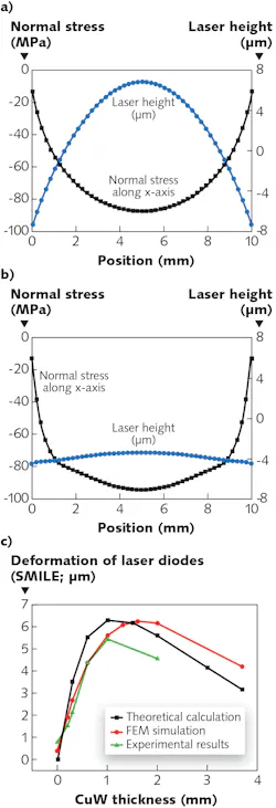
For digital-simulation modeling of this process, different packaging structures and materials were selected (see Fig. 3); the simulated results are shown in Figure 4a and 4b. A continuous-wave (CW) 200 W diode-laser bar with a thermal density of greater than 500 W/cm2 can be bonded on a microchannel cooler (MCC) heat sink. Thermal-dissipation capability should be considered in the simulation, as well as how to minimize the “SMILE” value. The finite-element model (FEM) simulation results show that the compression stress on the laser bar decreases with the increase of copper-tungsten (CuW) submount thickness, as the CuW submount works as a buffer layer and can thus absorb stress. However, the laser bar out-of-plane strain (SMILE value) is approximately zero when the diode-laser array is directly bonded onto the heat sink without a submount; the SMILE value is maximized when the thickness of the CuW submount is increased to 44% of the heat sink. Beyond this point, the SMILE value decreases with increasing CuW submount thickness. As seen in Figure 4c, the experimental results are well aligned with the simulation results.2 Therefore, the thickness of the submount affects the near-field nonlinearity of a laser bar significantly.
Simulation and modeling of heat in packaging of HPDLs
Scientific applications. Besides the SMILE, spectral width is also one of the key parameters of a diode-laser vertical stack. Improving the stack’s spectral performance is very important for increasing production yield, reducing costs, and enhancing competitiveness. For some scientific applications, narrow spectral width is especially important.Thermal design of HPDLs is critical, as a rise of junction temperature at the location of the p-n junction will adversely affect the output power, slope efficiency, threshold current, and lifetime of the device if the accumulated heat cannot be easily dissipated. Excessive heat can also cause spectral broadening and wavelength shift. Thermal management of HPDL devices has become a major challenge in laser design, manufacturing, and application.
In the design process for a vertical-stack laser, one of the main problems is the thermal crosstalk, which seriously affects the cooling efficiency. To avoid thermal crosstalk, a parallel liquid-cooling format is designed to overcome heat unevenness between the bars, effectively improving the thermal dissipation. Figure 5 shows the design of the parallel format of liquid cooling.
In the following case, the thermal design and structure optimization of a vertical-stack laser with more than 20 bars was simulated. The simulation results in Figure 6 show that most of the heat is dissipated via the cooling-flow liquid. There is no significant accumulation of heat and the temperature gradient of each bar is relatively uniform. The maximum temperature on the stack is 60.13°C.Based on the thermal simulation, the structure is optimized in many aspects, such as cooling-water flow rate, microchannel cooler design, and water distribution. The heat is taken away as quickly as possible by the cooling water, ensuring that no thermal accumulation exists between the bars.
Although the laser bars in vertical stacks are simultaneously conduction cooled and microchannel-liquid cooled, temperature nonuniformity remains among the bars due to thermal crosstalk and/or liquid flow nonuniformity. This nonuniformity can alter the wavelength of the bars and broaden the spectrum of the stacks.To achieve a very narrow spectral width, in our work, advanced packaging processes have been used to maintain uniformity of temperature distribution. First, total temperature distribution is simulated and calculated (see Fig. 7). Next, the wavelength of each bar is selected to match the temperature distribution based on the simulation results. The third and last step is to use optimized packaging technology to achieve the same output wavelength. Using this method, the spectrum broadening of a vertical stack can be effectively controlled.
Simulation and modeling of heat and stress in optical collimation microlenses
Optical collimation microlenses, including fast-axis collimators (FACs), slow-axis collimator (SAC) arrays, homogenizers, diffusers, collimators, beam transformation systems (BTS), and so on, are widely used in DPSS lasers, materials processing, 3D sensing, immersive photolithography, flexible display, lidar, and other application fields. These microlenses are commonly fixed on mechanical frames by adhesives. Controlling the stress on lenses and reduce the risk of cracks is therefore of great importance.A typical example is shown in Figure 8. A disastrous crack is found on a diffuser, although the adhesion is good. Simulation was carried out to look for causes of such cracks; the simulation results show that a higher stress, up to 61.58 MPa, occurred at one corner of the diffuser, which corresponds to the actual crack. After the adhesion in the FEA model was precisely controlled and the program run again, the stress on the diffuser decreased to 32.96 MPa, as shown in the figure. The result shows the benefit of FEM in improving adhesion processes.
Easy-to-use FEM methods have been presented for evaluating the thermal performance of HPDLs and the stress distribution in HPDLs. These methods make it much easier to understand the physics of the addressed thermal phenomena and predict their thermal behavior and performance. Digital-simulation modeling should be conducted before the manufacturing of HPDLs, helping to reduce R&D costs and quickly guiding engineers to the correct approach if thermal and stress distributions in a package are taken into account. The methodology described here for the application of diode-laser packages can also be used beyond this area of engineering for the analysis and design of packaging structures.
ACKNOWLEDGEMENT
DLight is a registered trademark of Focuslight Technologies.
REFERENCES
1. X. Liu et al., J. Appl. Phys., 100, 1, 013104 (2006).
2. H. Zhang et al., “High power 250 W CW conductively cooled diode laser arrays with low SMILE,” Proc. SPIE, 11261, 112610C (Feb. 2020).
3. C. Zah et al., “Low SMILE vertically stacked laser bars enable kW modular line lasers,” High Power Diode Lasers and System Conf. (Coventry, England), 9-10 (2017); doi:10.1109/hpd.2017.8261079.
Jingwei Wang is Chief Scientist, Tuanwei Fu is CAE Engineer, and Xuejie Liang is Manager of the Design and Simulation Technology Department, all at Focuslight Technologies, Xi’an, China; e-mails: [email protected], [email protected], and [email protected]; focuslight.com.


