Flexible high-volume die bonding solution targets modern photonics manufacturing
Global 5G deployment and datacenter applications over the next five years are expected to have exponential growth rates.1 This drives the demand for high-performance optical communication devices as one of the most critical building blocks. Specifically, these critical components are supporting 5G wireless fronthaul and the shipments of next-generation Ethernet modules, including 2x200GbE, 4x100GbE, and 400GbE, as well as CWDM/DWDM transceivers.2
This major market growth of new high-performance optical devices has generated new requirements, including much-smaller packaging housing, smaller chips/dies with higher density in the package, rapid technology innovation, quick product iterations, higher-volume manufacturing, and at an economical price point. The new requirements are also needed in lidar, AR/VR, and advanced photonic sensors, as well as MEMS and even the highly integrated silicon photonics devices.
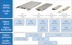
One of the greatest challenges in the manufacturing of these devices is the ability to successfully deploy flexible die bonding solutions to meet the wide range of needs for high-volume production with high post-bonding accuracy and great long-term stability.3 Historically, the post-bonding accuracy has been evolving from 10–15 µm to 7–10 µm, to 5–7 µm for each previous generation of photonic devices. The newest generations of high-performance photonic devices require a <3 µm post-bonding accuracy, without sacrificing high throughput or high flexibility for a high mix of product types in high-volume manufacturing.
The traditional high-volume semiconductor equipment may have high accuracy and high speed, but does not have the level of flexibility required for photonic devices. There also have been some die bonders specifically designed for photonics manufacturing with accuracy and flexibility or speed, but not all these criteria. Here, we introduce the industry-first field-proven post-bonding accuracy of 3 µm or better on a 1.5 µm high-speed and highly flexible die bonder platform (MRSI-HVM) for high-volume and high-mix photonics manufacturing.
High-volume, high-mix photonics manufacturing challenges
The developing trend in optical device assembly tolerance requires much higher post-bonding accuracy for new-generation optical devices with smaller assembly tolerances (see Fig. 1), necessitating higher-precision die bonder platforms. The post-bonding accuracy not only depends on the machine accuracy, but also depends on the chip/die and substrate materials tolerance, as well as process variations. The total assembly tolerance margin is very limited. The higher the machine accuracy and the smaller process variations, the higher the materials tolerance and higher-assembly process yield. To achieve <±3 µm post-bonding accuracy, the die bonding machine needs to have a stable <±1.5 µm machine accuracy. This <±1.5 µm @ 3 sigma accuracy, together with high-speed and high flexibility, has been a great challenge for die bonder machine suppliers.
Adding to this challenge is the demand for smaller and higher-density components, which can reduce the power consumption of the optical devices. The higher density components in the optical devices need the machine to provide the special high-precision top heating tools in case the neighbor chips/dies double-reflow during the eutectic process. This high-precision pulsed heating is very useful for the high-density optical devices, but it brings more challenges to the die bonder machines. In addition, unlike silicon electronics, photonics chips are usually very fragile, so the precise control of bonding force and height is also very critical.3
Comparing the business models of traditional telecom-centric business model and disruptive new cloud-based datacenters,4 the table illustrates the need for a large manufacturing base for the size of each order and a just-in-time ramp-up, as well as a cost-sensitive price point for the cloud-based datacenter (DC) model. This means the new cloud-based DC model needs something dubbed “elastic” high-volume manufacturing. In the 5G era, the 5G fronthaul is similar to the datacenter model and 5G backhaul is like the telecom model.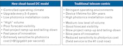
The long-term trend for optical devices in 5G is that they will be part of a high-mix, fast-growing market that has different bandwidth requirements, including the need for high-speed transceivers. Because of the rapid technology innovation and quick product iteration in the 5G and DC market, volume manufacturers will require a higher level of flexibility than in the past, which is a challenge for photonics device suppliers.
1.5 μm high-speed flexible die bonder
To meet these challenges, MRSI Systems (Tewksbury, MA) developed the MRSI-HVM die-bonder platform, which achieves < ±3 µm post-bonding accuracy at industry-leading speed with a high-level flexible die bonding process and long-term stability (see Fig. 2). This solution is targeted to support the latest high-volume flexible manufacturing for the photonics industry.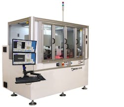
The die bonder itself has <±1.5 µm @ 3 sigma pick-and-place accuracy in order to achieve the post-bonding accuracy of <±3 µm @ 3 sigma. It deploys a dual-bonding heads/stages design with “on-the-fly” tool change to provide the high speed to fit different kinds of die-bonding process volume manufacturing in one machine.
Furthermore, this solution can also be a die bonding unit to support different kinds of die bonding processes in an optical device Flexible Manufacturing System (FMS) and the in-line system to link with other manufacturing units to achieve an Automated Intelligent (AI) factory.
MRSI-HVM is the only flexible high-speed die bonder that can achieve <±1.5 µm @ 3 sigma, and dozens of machines have been installed globally with outstanding results. It provides the best manufacturing solution for increasing volume and mix in manufacturing 5G and datacenter core devices.
Application test results
Standard glass dies are used to verify machine accuracy. During testing, 100 glass dies are picked and placed by the left-side head and right-side head for verifying both heads’ placement accuracy separately. Pick-and-place distribution results for the left and right heads show that both heads meet < ±1 µm @ 3 sigma accuracy (see Fig. 3). The platform has also achieved the same level of results for the configuration with a heated head on the right side.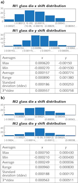
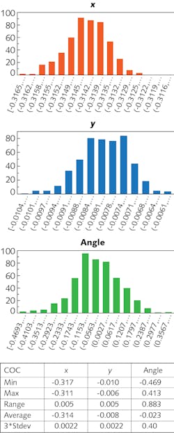
The post-bonding accuracy data demonstrates <±3 µm @ 3 sigma. The pick-and-place accuracy is the same as on a glass die for epoxy stamping configuration, except the post-curing shift is dependent upon individual process design by each customer. If in situ UV curing is used for epoxy processing, the post-curing accuracy can be <±3 µm @ 3 sigma as well. The machine achieves up to 1800 units per hour (UPH) depending on the application and has been running in production 24/7.
In summary, there are significant challenges facing high-performance optical communication device manufacturers driven by the requirements of 5G and datacenter applications. The high-volume, high-mix nature of the manufacturing requires single-assembly equipment that can deliver high accuracy, high throughput, high flexibility, and high stability concurrently. Field application results show MRSI’s innovative automation solution and MRSI-HVM series machines meet these challenges. Specifically, this system achieves the optical device “elastic” high-volume manufacturing requirements, and post-bonding <±3 µm @ 3 sigma goals with 1.5 µm machine accuracy in the production environment.
REFERENCES
1. See https://bit.ly/MRSIRef1.
2. See https://bit.ly/MRSIRef2.
3. Y. Qian, “Manufacturing Photonics: Challenges for photonics manufacturing in the new data center era,” Laser Focus World, 54, 8, 24–29 (Aug. 2018); https://bit.ly/MRSIRefer3.
4. L. Zhou et al., “High-power Laser Diodes: Die-bonder innovations target HPLD manufacturing challenges,” Laser Focus World, 56, 2, 21–24 (Feb. 2020); https://bit.ly/MRSIRefer4.
Dr. Limin Zhou is senior director of strategic marketing at MRSI Systems (Mycronic Group), Tewksbury, MA; e-mail: [email protected]; www.mrsisystems.com.
About the Author
Limin Zhou
Senior Director of Strategic Marketing, MRSI (Mycronic Group)
Dr. Limin Zhou is senior director of strategic marketing at MRSI Systems (Mycronic Group), Tewksbury, MA.