REDFINCH consortium grows mid-IR laser diodes on silicon towards low-cost sensors
For the first time, researchers have fabricated high-performance mid-infrared laser diodes directly on microelectronics-compatible silicon substrates. The new mid-infrared (mid-IR) lasers could enable the widespread development of low-cost sensors for real-time, accurate environmental sensing for applications such as air pollution monitoring, food safety analysis, and detecting leaks in pipes. The paper was published in Optica.
“Most optical chemical sensors are based on the interaction between the molecule of interest and mid-infrared light,” said research team leader Eric Tournié from the University of Montpellier in France. “Fabricating mid-infrared lasers on microelectronics-compatible silicon can greatly reduce their cost because they can be made using the same high-volume processing techniques used to make the silicon microelectronics that power cell phones and computers.”
The work was conducted at the EXTRA facilities and as part of the REDFINCH consortium, which is developing miniaturized, portable low-cost optical sensors for chemical detection in both gases and liquids.
“For this [REDFINCH] project, we are working upstream by developing photonic devices for future sensors,” said Tournié. “At a later stage, these new mid-infrared lasers could be combined with silicon photonics components to create smart, integrated photonic sensors.”
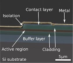
For about a decade, the researchers have been working on depositing III-V semiconductor material on silicon using a method known as epitaxy. Although the researchers previously demonstrated lasers on silicon substrates, those substrates were not compatible with industry standards for microelectronics fabrication. When using industry-compatible silicon, differences in the material structures of the silicon and the III-V semiconductor cause defects to form.
“A particular defect called an anti-phase boundary is a device killer because it creates short-circuits,” said Tournié. “In this new work, we developed an epitaxial approach that prevents these defects from reaching the active part of a device.”
The researchers also improved the process used to fabricate the laser diode from the epitaxial material. As a result, they were able to create an entire laser structure on an industry-compatible silicon substrate with a single run of an epitaxial tool.
The researchers demonstrated the new approach by producing mid-infrared laser diodes that operated in continuous-wave mode and exhibited low optical losses. They now plan to study the lifetime of the new devices and how that lifetime relates to the fabrication and operation mode of the devices.
They say that once their method is fully mature, epitaxy of lasers on large silicon substrates (up to 300 mm across) using silicon microelectronics tools will improve control of the fabrication process. This will, in turn, further reduce laser fabrication costs and enable the design of new devices. The new lasers could also be combined with passive silicon photonics integrated circuits or CMOS technology to create small, low cost, smart photonic sensors for gas and liquid measurements with high sensitivity.
“The semiconductor material we work with allows fabrication of lasers or photodetectors operating in a broad spectral range, from 1.5 microns (telecom band) to 25 microns (far infrared),” said Tournié. “Our fabrication method can be applied in any field where one needs to integrate III-V semiconductors on silicon platforms. For example, we have already fabricated quantum-cascade lasers emitting at 8 microns by applying this new epitaxial approach.”
SOURCE: Optica; https://www.osapublishing.org/optica/abstract.cfm?uri=optica-7-4-263
About the Author

Gail Overton
Senior Editor (2004-2020)
Gail has more than 30 years of engineering, marketing, product management, and editorial experience in the photonics and optical communications industry. Before joining the staff at Laser Focus World in 2004, she held many product management and product marketing roles in the fiber-optics industry, most notably at Hughes (El Segundo, CA), GTE Labs (Waltham, MA), Corning (Corning, NY), Photon Kinetics (Beaverton, OR), and Newport Corporation (Irvine, CA). During her marketing career, Gail published articles in WDM Solutions and Sensors magazine and traveled internationally to conduct product and sales training. Gail received her BS degree in physics, with an emphasis in optics, from San Diego State University in San Diego, CA in May 1986.