VCSEL Advances: VCSEL power-conversion efficiency improves to 45%
GERALD DAHLMANN, VIPUL BHATT, and SANJAI PARTHASARATHI
Over the last few years, advances in laser technology originally developed for optical communications are now being leveraged in other high-volume market verticals, including consumer electronics. The vertical-cavity surface-emitting laser (VCSEL) heritage extends back to the pioneering work of Professor Iga1 in the mid-1970s, who first demonstrated the device structure, followed by Jack Jewell and his team at Bell Laboratories, who in the late 1980s fabricated one million VCSEL die on a single wafer.2
Since then, VCSELs have been adopted in a significant number of important applications, including illumination for infrared imaging, thermal heating and curing, optical encoders, atomic clocks, oxygen sensors, optical touchpads, computer mice, printers, and driver monitoring systems in automobiles. They have been widely adopted in optical communication systems and more recently in 3D sensing.
Among the various new applications for VCSELs, 3D sensing is undoubtedly one of the recent commercial successes making a great impact on the industry. With the advent of face biometrics in smartphones, 3D sensing and VCSELs have become part of our daily lives. Many of the advances made in VCSEL technology over the past five years have been driven by the demand from well-known brands in consumer electronics that integrate 3D cameras into their smartphones and tablets.
3D sensing
Within 3D sensing, two fundamentally different techniques are being used: triangulation and time-of-flight (ToF). For triangulation, one technique called structured light consists of projecting a light pattern into the scene and reconstructing in 3D the distortions of the pattern when measured from a slightly different perspective. For ToF, the time delay between an outgoing light pulse and the detection of the resulting backscatter is used to reconstruct the 3D scene.
At a high level, the requirements for VCSELs are similar for both techniques. A longer wavelength of 940 nm is preferred, compared with the more-typical datacom wavelength of 850 nm that can emit a visible red glow. On the detector side, operation at 940 nm offers the best tradeoff between the quantum efficiency of CMOS image sensors and signal-to-noise ratio in the presence of background sunlight. Both triangulation and ToF benefit from the VCSEL’s inherent narrow spectral width and low wavelength drift over temperature. Both techniques also require high power-conversion efficiency to minimize power consumption and self-heating.
There are, however, important differences between VCSEL arrays for triangulation-based and ToF-based systems. For triangulation, the measured signal is in the spatial domain, driving high uniformity requirements across VCSEL arrays and stringent beam parameters for individual VCSEL emitters in each array. On the other hand, for ToF, the measurement is in the time domain, requiring fast switching and control over the temporal shape of the VCSEL array output to generate pulses with short rise and fall times.
The demand for higher performance in 3D sensing will drive diverging requirements for triangulation and ToF techniques. Promising developments in VCSEL technology, including power-conversion efficiency, single-mode beams, and flip-chip-mounted designs, may be significant factors enabling next-generation 3D sensors.
Power-conversion efficiency
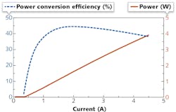
Power-conversion efficiency is a key metric for VCSEL arrays used in mobile devices, which are battery-powered and for which dissipation of excess heat can be a great challenge. Next-generation 3D sensors will have a higher pixel count and longer range and will therefore consume even more power. Recently, II-VI has significantly improved VCSEL power-conversion efficiency to 45% at 50°C operating temperature (see Fig. 1). Development efforts are ongoing with the objective of achieving a power-conversion efficiency of greater than 50%.
Single-mode VCSELs offer advantages for ToF 3D sensing, as they can be switched on and off at very high speeds. In addition, single-mode emitters have a Gaussian beam profile and low divergence, which enable more-efficient and lower-cost optics at the module assembly level. For structured light systems, the lower divergence results in smaller dot size, allowing higher spatial resolution. II-VI is driving the development of single-mode VCSELs to achieve output power levels that are comparable to the output of today’s multimode VCSELs.
Flip-chip-mounted VCSELs eliminate parasitic inductance from bond wires, significantly increasing the VCSEL speed and reducing assembly time.
Optical communications
In optical communications, VCSELs operating at 850 nm enable high-speed transceivers and active optical cables for datacenters and high-performance computers. These VCSELs operate at up to 56 Gbit/s (50G), enabling a range of datacom transceivers such as 200G-SR4 (4 lanes of 50 Gbit/s each), 400G-SR4.2, and 400G-SR8 (8 lanes of 50 Gbit/s each).
For datacom applications, VCSELs offer several significant advantages. Their circular beam shape and low divergence angle allow for efficient coupling into multimode fibers. Their vertical cavity structure is such that the laser beam travels perpendicularly to the plane of the wafer, which allows wafer-level testing of the optical performance of each laser and greatly improves the yield of assembled devices and modules. Compared with edge-emitting lasers, VCSELs are smaller in size, which allows faster direct-modulation speeds. The combined advantages of low power dissipation, high density, and low cost are why transceivers based on VCSELs remain the technology of choice for datacenter links spanning up to 300 m, despite ongoing investments in alternative technologies such as silicon photonics.
As to whether VCSELs can enable the next higher speed of 100 Gbit/s, the answer is a resounding yes. In November 2019, the IEEE 802.3 Working Group unanimously supported the formation of a study group to develop objectives for 100G short-reach optical interconnects, mainly aimed at datacenter applications.3 Using PAM4 modulation, VCSEL performance (see Fig. 2) can be increased from 50 Gbit/s today to 100 Gbit/s per lane (50 GBaud PAM4).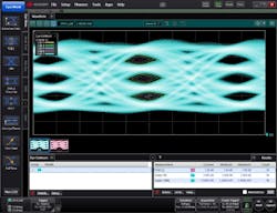
Optical transceivers based on these higher-speed VCSELs, when combined with multiple fiber pairs or multiple wavelengths per fiber pair, are expected to support the growing bandwidth needs of datacenters for the foreseeable future.
High-volume manufacturing of VCSELs
The benefits of VCSELs over edge-emitters for short-reach datacom transceivers are directly applicable to high-volume applications in consumer electronics. In addition, VCSELs can be arranged in two-dimensional arrays to scale the output power, resulting in a larger die size. The combination of higher volumes and larger die sizes required for 3D sensing VCSELs in face biometrics applications has recently driven the scaling of II-VI’s underlying gallium arsenide (GaAs) technology platform from 100 mm to 150 mm wafer diameters.
Concurrently, wafer-level testing of VCSELs has advanced and enabled significant improvements in production uniformity and quality. Measurement techniques were also developed specifically to generate the data required by customers who need to ensure that VCSEL assemblies are eye-safe in end-user applications.
In-line quality control of VCSELs in a modern manufacturing line does not end with wafer probe testing. Once the wafers are diced, the front and back side of the chips are optically inspected to meet the requirements for workmanship. Each wafer lot is further validated through a rigorous environmental stress test to ensure that the VCSELs will maintain a high level of reliability, even in the most challenging end-user environments.
Thanks to 3D sensing, II-VI shipments of VCSEL emitters have seen a 70% annual growth rate since 2017. The rapidly growing demand was met by leveraging a vertically integrated in-house manufacturing footprint across five modern facilities, including four in the U.S. and one in Europe.
Conclusions
Over the past five years, the mass adoption of VCSELs in mobile phones and optical links for datacenters has accelerated innovation cycles and led to dramatic improvements in the technology. Each new generation of VCSELs is designed to be faster, more efficient, and more reliable than the last. Significant investments in innovation have enabled the scaling of the GaAs technology platform to 150 mm, which is now the state of the art. The next five years will bring more innovation as the demand for VCSELs increases further, driven by the growing bandwidth needs for datacenters, cloud computing, and 5G wireless connectivity, and the adoption of 3D sensing in exciting new applications such as augmented reality.
REFERENCES
1. H. Soda, K. Iga, C. Kitahara, and Y. Suematsu, Jpn. J. Appl. Phys., 18, 12, 2329–2330 (1979).
2. J. L. Jewell et al., Appl. Phys. Lett., 51, 2, 94–96 (1987).
3. See http://bit.ly/IIVIRef3.
Gerald Dahlmann is Director of Strategic Marketing, Consumer Electronics at II-VI, Zurich, Switzerland; Vipul Bhatt is Senior Director of Strategic Marketing, Datacom at II-VI, Sunnyvale, CA; and Sanjai Parthasarathi is Chief Marketing Officer at II-VI, San Jose, CA; e-mail: [email protected]; www.ii-vi.com.