Single-layer OLED design could dramatically reduce display costs
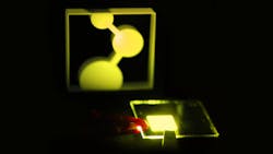
Organic light-emitting diodes (OLEDs) are used today in many electronic devices for display applications, ranging from smartphones to televisions. Scientists at the Max Planck Institute for Polymer Research (MPI-P; Mainz, Germany) have now succeeded in developing a new design for these LEDs. Described in Nature Photonics, they have been able to reduce the number of different layers that make up an OLED to just one. In the future, this could allow LEDs that can be printed with an inkjet printer and dramatically lower display costs and complexity. The first prototype of the developed diode can already compete with current, commercially available OLEDs in terms of luminosity and efficiency.
Today, OLEDs no longer consist of compounds containing the semiconducting material gallium, but of so-called organic compounds in which carbon is a main component. Compared to conventional LEDs, however, the luminosity and lifetime of OLEDs are currently lower.
Scientists at the MPI-P led by group leader Gert-Jan Wetzelaer (department of professor Paul Blom) have now developed a new OLED concept. Nowadays, OLEDs consist of various wafer-thin layers. Some layers are used to transport charges, while others are used to efficiently introduce electrons into the active layer in which light is generated. Thus, current OLEDs can easily consist of five to seven layers. The researchers have now developed an OLED that consists only of one single layer that is supplied with electricity via two electrodes. This simplifies the production of such OLEDs and paves the way for printable displays.
With their first prototype, the Mainz scientists were able to show that they can generate a brightness of the emitted light of 10,000 candela/square meter with a voltage of only 2.9 volts - this corresponds to about 100 times the luminosity of modern screens. Achieving such high luminosity at this low voltage is a record for current OLEDs. The researchers were also able to measure an external efficiency of 19%, which means that 19% of the electrical energy supplied is converted into light that comes out in direction of the viewer. Also with this value, the OLED prototype can compete with current OLEDs consisting of five or even more layers.
In continuous operation, the researchers were able to measure a so-called LT50 lifetime of almost 2000 hours at a brightness equivalent to ten times that of modern displays. Within this time, the initial luminosity has dropped to 50% of its value.
"For the future, we hope to be able to improve the concept even further and thus achieve even longer lifetimes. This means that the concept could be used for industrial purposes," says Wetzelaer. The scientists hope that their newly developed single-layer concept will contribute to the identification and improvement of the processes responsible for the reduction in luminance over time.
The scientists are using a light-emitting layer based on so-called “thermally activated delayed fluorescence” (TADF). This physical principle has been known for several decades, but became the focus of OLED research about 10 years ago, when an efficient conversion of electrical energy into light was demonstrated in Japan. Since then, researchers have been working to produce TADF-based OLEDs, as these do not require expensive molecular complexes containing rare-earth metals that are being used in current OLEDs, significantly reducing cost.
SOURCE: Max Planck Institute for Polymer Research; https://www.mpip-mainz.mpg.de/presse/pm-en-2019-09
About the Author

Gail Overton
Senior Editor (2004-2020)
Gail has more than 30 years of engineering, marketing, product management, and editorial experience in the photonics and optical communications industry. Before joining the staff at Laser Focus World in 2004, she held many product management and product marketing roles in the fiber-optics industry, most notably at Hughes (El Segundo, CA), GTE Labs (Waltham, MA), Corning (Corning, NY), Photon Kinetics (Beaverton, OR), and Newport Corporation (Irvine, CA). During her marketing career, Gail published articles in WDM Solutions and Sensors magazine and traveled internationally to conduct product and sales training. Gail received her BS degree in physics, with an emphasis in optics, from San Diego State University in San Diego, CA in May 1986.