CEA-Leti develops CMOS wafer-based microLED fabrication technique

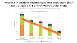
IMAGE: MicroLED displays are forecast to be big business, with cost reduction through improved fabrication methods a requirement for large-scale commercialization. (Image credit: Yole Developpement)
Leti (Grenoble, France), a research institute of CEA Tech, announced a new technology for fabricating gallium nitride (GaN) microLED displays for applications ranging from smart watches to TVs with no size limit. The approach fabricates elementary units of all-in-one red, green, blue (RGB) microLEDs on a CMOS driving circuit and transfers the devices to a simple receiving substrate. The units are fabricated with a full semiconductor, wafer-scale approach.
“This new process, in the proof-of-concept stage, paves the way to commercial, high-performance microLED displays,” said François Templier, CEA-Leti’s strategic marketing manager for photonic devices. “The CMOS-based approach provides higher brightness and higher resolution microLEDs and is a game changer for very large TVs.”
While they promise exceptional image quality and better energy efficiency than existing liquid crystal display (LCD) and organic light-emitting diode (OLED) technologies, microLED displays currently face significant barriers on the road to commercialization.
One of the biggest challenges is improving the performance of the driving electronics, which require more power to deliver brighter images and more speed to support continuously increasing demands for high display resolution. Faster electronics are required to power millions of pixels in a fixed-frame time in microLED displays, but existing driving display technology, known as thin-film transistor (TFT) active matrix, cannot provide the necessary current and speed.
CEA-Leti’s new approach fabricates CMOS-driven, high-performance GaN microLED displays with a simplified transfer process that eliminates the use of the TFT backplane. RGB microLEDs are stacked directly onto a micro-CMOS circuit, and each unit is transferred onto a simple receiving substrate. Then, the RGB microLEDs and the backplane are fabricated on a single semiconductor line.
In addition to increasing power and driving speed--and improving display performance--this process avoids several costly steps needed with current technology to make electrical and mechanical contacts between microLEDs and the receiving substrates. CEA-Leti presented a paper on the breakthrough titled “A New Approach for Fabricating High-Performance MicroLED Displays” on May 14, during Display Week 2019 in San Jose, CA.
SOURCE: CEA-Leti; http://www.leti-cea.com/cea-tech/leti/english/Pages/What's-On/Press%20release/MicroLEDs-That-Could-Overcome-Display-Size-Obstacles-.aspx
About the Author

Gail Overton
Senior Editor (2004-2020)
Gail has more than 30 years of engineering, marketing, product management, and editorial experience in the photonics and optical communications industry. Before joining the staff at Laser Focus World in 2004, she held many product management and product marketing roles in the fiber-optics industry, most notably at Hughes (El Segundo, CA), GTE Labs (Waltham, MA), Corning (Corning, NY), Photon Kinetics (Beaverton, OR), and Newport Corporation (Irvine, CA). During her marketing career, Gail published articles in WDM Solutions and Sensors magazine and traveled internationally to conduct product and sales training. Gail received her BS degree in physics, with an emphasis in optics, from San Diego State University in San Diego, CA in May 1986.