Dual-sided laser processing can tap static beam shaping and splitting
Simultaneous laser processing of opposite sides of a substrate presents significant opportunities to improve throughput in manufacturing. Our conceptual static optical beam shaping setup operates simultaneously on both sides of a substrate using a single laser and optical system—without moving parts.
We integrated diffractive beam splitting with top-hat beam shaping and dual-sided focusing, and optical simulations in Ansys OpticStudio validate the feasibility of our approach for various laser applications, including continuous wire processing, semiconductor wafer scribing, and solar cell inspection.
While most laser processing systems operate on a single surface at a time, many applications could benefit from simultaneous access to opposite sides of a workpiece. Current solutions typically require complex mechanical repositioning or multiple laser setups, which adds cost and cycle time.
Diffractive optical elements (DOEs) are established tools for beam shaping and splitting in industrial laser applications.1 Recent advances in 3D beam shaping demonstrated the ability to control intensity distributions in 3D space.2,3 Building upon these developments, we present a novel optical configuration that combines diffractive beam splitting with dual-sided focusing to enable simultaneous laser processing on opposite sides of a substrate, using Holo/Or’s DOEs.
Optical design concept
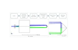
Our approach uses a diffractive beam splitter to divide the incident laser beam into two beams, which are then directed by static mirrors to opposite sides of the workpiece. Figure 1 illustrates the system architecture from optical simulation, while Figure 2a shows a 3D rendering of the physical implementation.
The optical path consists of:
Input beam. Single-mode Gaussian laser beam (λ = 355 nm, 3.2-mm diameter at e-2).
Line top-hat beam shaper. Converts Gaussian profile into uniform top hat distribution.
Diffractive beamsplitter (double-spot DOE). Splits beam into two identical beams with defined separation angle.
Telecentric F-theta lens (EFL = 100.2 mm). Focuses both beams while maintaining near-normal incidence.
Folding mirrors. Positioned so focal planes coincide with opposite substrate sides.
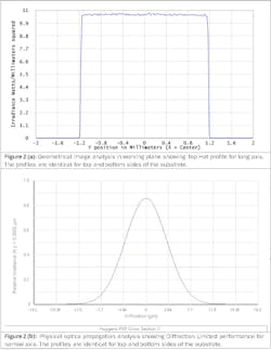
Our optical design was validated by Ansys OpticStudio simulations. Key performance parameters derived from the simulation results (see Fig. 2) were: Output spot geometry of 2.3 mm × 0.014 mm (line profile); uniformity: >90% within the top-hat region; and efficiency: >78% (accounting for all optical losses).
Key potential industrial applications
Figure 3 shows the physical system and schematic configurations for key applications:
Continuous wire processing. One of the most promising applications is continuous wire processing, in which wire feeds through the system and both diametrically opposite surfaces are treated simultaneously without requiring wire rotation (as shown in Fig. 1b).
Magnet wire (enameled wire). Removal of enamel coating from wire ends during cutting operations. Used in billions of meters annually for electric motors and transformers, particularly relevant for electric vehicle (EV) motor production. Current thermal or mechanical stripping methods are slower and can damage wire dimensions. This dual-sided approach provides complete circumferential coating removal without wire rotation, which enables inline processing.
Medical guidewires. Surface preparation of fine wires (0.1 to 1.0-mm diameter) for catheter applications. Noncontact dual-sided processing avoids mechanical handling damage while enabling complete circumferential treatment, which is critical where dimensional tolerances directly impact device performance.
Fiber-optic cables. Removal of protective coatings from optical fibers (125 to 900 μm) before splicing. Dual-sided laser ablation reduces fiber cracks common with mechanical strippers, critical for telecom and data center applications, while ensuring complete circumferential coating removal.
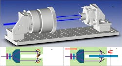
Figure 1c shows a configuration for wafer-level applications scalable to different sizes by selecting appropriate F-theta focal lengths. For example, a 300-mm focal length system provides coverage for 200- to 300-mm wafers with spot sizes of 10 to 50 μm for scribing.
Double-sided scribing. Silicon wafers for power semiconductors and solar cells require scribe lines on both surfaces for controlled cleaving. Simultaneous scribing provides front-to-back alignment while eliminating wafer flipping, improving throughput. Symmetric scribing may also improve cleave quality and reduce edge chipping.
Inspection applications. The dual-sided line configuration enables simultaneous optical inspection of both surfaces for bifacial solar cells and thinned semiconductor wafers, and potentially increases inspection throughput. It also reduces handling and enables correlation of defects between surfaces.
Concept versatility
The optical setup can be modified for custom specifications such as:
Multi-beam configurations. The double-spot splitter can be replaced with multibeam elements (3, 4+ beams) for processing from multiple angles or creating redundancy.
Dynamic scanning. Static mirrors can be replaced by galvo scanners for extended area coverage and pattern generation.
Flexible beam shaping. The line shaper can be replaced by circular top hat, rectangular, or custom profiles depending on application requirements. For applications requiring tight focusing (such as wafer scribing), the beam shaper can be omitted entirely to achieve diffraction-limited spot sizes.
Adjustable working envelope. System accommodates different substrate thicknesses (0.5 to 10+ mm typical) by repositioning mirrors.
Scalable architecture. System is scalable to different working envelopes by selecting appropriate F-theta focal lengths (100 to 300 mm typical) while maintaining high-quality focusing performance.
Wavelength flexibility. Concept is wavelength-agnostic and applicable to ultraviolet (UV), visible, infrared (IR), and ultrashort-pulse lasers.
Inspection integration. For inspection applications, cameras or detectors can be integrated to capture images or signals from both sides simultaneously, with the laser providing line illumination.
We believe this approach combined with Holo/Or’s diffractive optical elements shows potential to enable efficient and economical manufacturing solutions. Its modular design allows extensive customization for specific applications, wavelengths, and power levels. Further experimental work is needed to validate these concepts and explore their practical implementation.
REFERENCES
1. A. Völl, J. Stollenwerk, and P. Loosen, Laser Tech. J., 15, 1, 42–45 (2018).
2. J. Meinschien, C. Stauch, T. Schubert, and S. Hellstern, PhotonicsViews, 19, 5, 48–51 (2022); https://doi.org/10.1002/phvs.202200037.
3. S. Gräf and F. A. Müller, Sci. Rep., 11, 22944 (2021); https://doi.org/10.1038/s41598-021-02290-3.
About the Author
Alexander Brodsky
Alexander Brodsky is a senior optical designer at Holo/Or (Rehovot, Israel).
Natan Kaplan
Natan Kaplan is CTO and R&D manager at Holo/Or (Rehovot, Israel).
Shmuel Cohen
Shmuel Cohen is an optomechanical designer at Holo/Or (Rehovot, Israel).