Ultraprecise high-speed laser processing of large substrates

Every large glass substrate, whether used as architectural or functional glass within the solar industry or for manufacturing semiconductors or flat screens, is always a combination of two components: a substrate glass and at least one coating.
Two processes are used for these substrates: selective coating or selective removal of full-surface functional coatings. This article explores the ultrafast laser ablation or functionalization of defined layers of large substrates.
The trend toward high-density features or full-surface texturing in conjunction with fast-moving panels or web-based applications challenges established laser scanning solutions. Where lasers can provide satisfactory performance, the traditional approach of multiplexing systems seems to be the way forward. To support and deliver laser material processing on a full industrial scale, LPKF SolarQuipment and the SCANLAB polygon team developed a system concept for validating the process and identifying the control features that need to be tailored. It supports double-sided (top-bottom) synchronized processing of preregistered patterns of thin film on glass.
Wafer and panel processing
The solar, semiconductor, and flat-panel display industries are high-volume manufacturing industries that need to process large areas with high accuracy (see Fig. 1). The larger scan field size compared to conventional scan heads, combined with the improved pulse repetition rate and higher average power of ultrafast and the latest nanosecond-pulsed lasers, makes it possible to process larger areas with a higher throughput.
For ultraprecise processing of large areas using transmissive f-theta optics, a step-and-repeat approach can be taken. This approach introduces challenges with respect to stitching (overlap of different scan passes).
Ultraprecise micromachining requires small, focused spot sizes and a full telecentric field of view—for example, a constant round spot over the entire scan area. But traditional refractive optics using lenses are limited in size because of the progressive increase in cost with the increasing image field. This means cost-efficient, highly accurate laser scan heads with refractive f-theta optics have limited scan fields.
An alternative solution for avoiding stitching is wide-field mirror optics. The core technology for this is a polygon scanner system with integrated f-theta mirror optics. It uses a scan head with a full telecentric scan field of 300 mm and has a scan field 4–5X wider than that of conventional f-theta optics. Such a large width eliminates stitching for processing of wafers of up to 300 mm in size. Multiple scan heads can be mounted side by side to achieve panel size (1200 mm; see Fig. 2).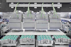
Choice of laser source
Depending on the coating and desired scribing result, different laser sources can be used. Processing direction, wavelength, and pulse frequency are optimized for the respective coating to yield optimal cost/performance/quality.
Because the LPKF systems can place laser units on the top and bottom sides, multilayer structures with layers composed of different materials can also be processed.
Quality aspects of LPKF laser scribing
The challenges to achieve a stable production process are manifold. Ultimately, optimal results (quality) and the lowest possible cycle time flow into the economic evaluation of the production process.
The following are influencing factors:
- For precise stitching with multiple polygon scanners, numerous factors including seed clock frequency, laser jitter, and a temperature-controlled system housing play a role in reducing tolerances down to the micron range.
- Synchronization of individual processing units is accomplished through a master/slave controller and active correction with the help of integrated sensors. A further aspect is spatial offset of individual units in the feed plane and the asynchronous control of individual processing units.
- Calibration of a multihead scanner is a daunting task. It is accomplished via integrated monitoring of the entire substrate based on preregistration, recording of temperature effects, recording of glass flatness, and continuous checking of the PU-specific scribing results. These values are converted to optimized scribing values in the control module.
Through these complex measures, a high-quality level is secured, even with high throughputs. The interplay between the coupled processing units is set by the presented measures such that the transitions between the individual scan fields are only a few microns in width.
Overall performance of LPKF processing
Processing speed plays the most important role after quality. It determines the cycle times and profitability of the process.
The first decisive value is the speed with which the scanners move the laser beam over the material. Here, up to 170 m/s is achieved over a scan width of 300 mm with each system.
Comparable galvo scanners can only generate scan fields of up to 100 mm and reach speeds of up to 40 m/s—the polygon scanner has an aspect ratio of 1:3 compared with galvo scanners. The polygon technology has a huge throughput advantage, especially for applications with high fill factors. Added to this is a lower cost of ownership due to the aspect ratio of 1:3, with a simultaneously higher uptime due to the reduction in the number of processing units.
A demonstrator system for process development is available at the LPKF application center. First article inspections of substrates with sizes of up to 1.2 × 1.2 m are possible.
LPKF SolarQuipment (Suhl, Germany) is a provider of systems for structuring thin film solar cells with large-format laser scribers. Its laser scribers have all the necessary components for highly dynamic glass handling, inline inspections, and control.
SCANLAB has been developing and manufacturing galvanometer scanners and scan solutions since its founding in 1990. SCANLAB’s products turn lasers into precise, highly dynamic, and flexible tools that provide the basis for performing countless processing tasks.
About the Author
Holger Schlüter
Head of Business Development, SCANLAB GmbH
Dr. Holger Schlüter is Head of Business Development at SCANLAB GmbH (Puchheim, Germany).
Stefan Freudenberg
Project Manager, LPKF
Stefan Freudenberg is project manager at LPKF (Garbsen, Germany).