Multibeam laser marking: The individual traceability enabler
Customer engagement, anticounterfeiting, brand protection, tracking, and tracing along the supply chain are industry-wide concerns. There are individual product traceability applications that benefit every actor in the value-chain. Consumers caring where their food comes from, a medical laboratory fighting forgery to protect public health, manufacturers optimizing operational efficiency to relocate production—all will benefit from the exceptional ability of 2D barcodes1 to convey information.
The move toward a globalized and digitally connected world, combined with consumers searching for more control and transparency, is creating an unprecedented demand for individual product traceability across various industry sectors. While data management infrastructures and services are now largely available,2 the key challenge for brands and manufacturers resides in how to individually identify their products.
Standard industrial marking solutions fail to deliver in an increasing number of cases because they cannot combine precision, throughput, and quality. Wireless techniques, such as near-field communication (NFC), are attractive, but costly to implement on a large scale. The ecological footprint of the marking solution is to be considered, too, particularly when it involves inks, coatings, and solvents.
Laser marking is one step in the right direction.
Standard laser marking
Contactless, consumable-less lasers can directly mark most packaging materials permanently.
For standard marking applications, three laser technologies prevail: the carbon dioxide (CO2) gas laser emitting in the shortwave-infrared (SWIR), the fiber laser operating in the near-infrared (NIR), and solid-state lasers operating in the visible or UV. Laser wavelength is determined according to the target material, and power according to the marking speed. The laser is then combined to a galvanometric scanning system (scanner) to form a laser marker.
For the laser industry, throughput is historically equivalent to laser beam movement speed—like moving a pencil faster to write faster. More throughput is always welcomed, and the laser industry’s answer was to provide higher laser power, higher pulse repetition rate, and faster scanning mirrors. But today, the marginal investment to further increase speed is becoming prohibitive for many users, from both a cost and complexity point of view.
Today, standard laser marking systems are seriously challenged by the breadth of new use cases, where it fails to deliver enough throughput for various reasons:
The markings are too small. Below 3 mm, laser markers operate in a nonefficient regime because the mirrors are constantly battling inertia, moving back and forth over very small distances.
The target object is moving too fast. Laser marking on a moving object is called “marking on the fly” (MOTF). It requires expensive electronics to drive the scanner, which must compensate the linear movement of the object while marking. MOTF often comes with degraded marking quality up to the maximum line speed of ~100 m/min.
The material has challenging surface characteristics. Materials such as polymers or glass are notoriously difficult to laser-mark at high throughput. Polymers might require using low power to avoid deleterious effects like burning; glass has a very high marking threshold and tendency toward microcracks, which causes quality issues.
The current paradigm is finding its limits. What about considering a shift or, at least, an opening?
A breakthrough innovation: multibeam laser marking
In the 15th century, Gutenberg invented the printing machine. In the three years needed to write one bible, 180 could be printed. The consequence was a massive spread of information throughout Europe, as well as faster and wider education, which eventually contributed to the Siècle des Lumières, also known as the Age of Enlightenment.
The concept of multibeam laser marking is similar: the “pencil” laser beam is replaced by a printing array of beamlets (see Fig. 1). Dozens of beamlets are marking the object simultaneously, stepping up the throughput dramatically. In this case, however, the printing machine would be digital because these beamlets are dynamically generated and individually controlled by software.
At the heart of this system are optoelectronical components called liquid-crystal-on-silicon spatial light modulators (LCOS-SLM). These are special liquid-crystal displays (LCDs) used as mirrors to reflect laser beams. When light shines on them, each pixel is electronically controlled to locally modulate an invisible property of light called “the phase.” This phase modulation is like a virtual hologram, which patterns the light intensity at the focus of the focusing lens.
Applying LCOS-SLM to industrial applications, in particular high-power applications such as laser marking, requires in-depth understanding and experience of:
- Laser-matter interaction: a necessary starting point to define a good marking solution.
- Algorithmic: the special programming required to manipulate light in the proper way; this is a major contributor to multibeam laser marking performance.
- Optomechanical design: a special blend of both Gaussian and ray-tracing design theories is required.
- LCOS-SLM technology: to select adequate performance and define reliable operation windows.
Multibeam laser marking applications
Applications are based on two methods—FULL-STAMP3 marking and PIXEL-STAMP4 marking. Here, we present FULL-STAMP marking.
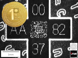
FULL-STAMP marking offers high-throughput microcodes for industrial use. Microcodes designate data matrix codes with a size typically ranging from 500 µm to 3 mm.
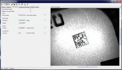
Microcodes are dedicated to professional applications because they require a specific, simple reading system. Microcodes are used to identify small and valuable parts, including PCB components, or to add discrete traceability information, which is an elegant and effective anticounterfeiting solution for brands.
The main feature of microcodes is their small size. Standard laser marking typically fails to deliver in this region because of inertia. On such a small scale, galvanometric scanners moving mirrors never work in an efficient regime because they are constantly moving back and forth.
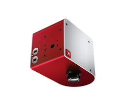
Multibeam laser marking is particularly good at marking microcodes. Using the patented FULL-STAMP marking approach, a microcode is marked with a single pulse. The VULQ1, for example, turns the input laser beam into a matrix of beamlets called “beam pattern,” representing the data matrix code, alphanumeric characters, or picture to be marked (see Fig. 3).The beamlets composing the beam pattern hit the material simultaneously, stamping the code in a permanent manner directly onto the surface within a few nanoseconds. Then, software changes the beam pattern within a few tens milliseconds to serialize the next product with the next laser pulse.
Benefits of FULL-STAMP marking include:
- Marking rate: 20 unique codes per second for serialization and 1000 codes per second for lot marking.
- Superior code quality: the whole code is marked at once, which ensures a perfect geometry despite the small size.
- Straightforward integration on fast moving lines: the only requirement is to shoot on the target location; there is no need for costly electronics.
- Maximal efficiency: single pulse marking minimizes heat loss into the material, which is a benefit for sensitive parts.
In a MOTF situation, multibeam marking seamlessly delivers perfect quality at several hundred meters/min. At 500 m/min, the target object travels 0.05 µm during the few nanoseconds required to mark the whole code. Only a simple synchronization scheme is required to shoot at the right position. Modern industrial DPSS lasers have a typical jitter of ≤1 µs, corresponding to <10 µm code positioning accuracy.
The major disadvantage of FULL-STAMP marking is that it isn’t applicable to every situation. The scope of application is limited by the maximum energy specified for the VULQ1 multibeam-shaping system, a critical parameter to ensure reliable operation.
For customer applications involving large QR codes or to mark transparent materials such as glass packages, the PIXEL-STAMP marking solution offers the best of the multibeam and scanning worlds.
Conclusion
With increasing global regulations and consumer demand for more transparency, manufacturers need solutions that provide visibility along the supply chain. In an increasingly competitive consumer market, brands need solutions to directly address their customers and protect themselves against counterfeiting. Individual product traceability is a ready solution.
Multibeam marking enables individual product identification in many situations where it is not currently possible with standard industrial marking techniques. It leverages the potential of process parallelization for industrial marking, joining forces with digital technologies to offer a breadth of new possibilities to brands and manufacturers.
The digitization of our way of consumption is a global trend coming along with major opportunities. Are you ready to seize them?
REFERENCES
1. Most common 2D codes are data matrix for B2B applications and QR codes for B2C applications.
2. See https://bit.ly/3x0IWkG.
3. See https://bit.ly/3Kf1WPZ.
4. Patent pending
5. See https://bit.ly/3x6yTdZ.
About the Author
Florent Thibault
President and CEO, QiOVA
Dr. Florent Thibault is president and CEO of QiOVA (Andrézieux-Bouthéon, France). Before joining QiOVA, Florent worked as Product Line Manager of Industrial Picosecond Lasers lines for Coherent in Germany, where he had global ownership of product lines like HyperRapid NX or Rapid NX. He also worked for Teem Photonics (Grenoble, France), a passively Q-switched laser business, where held various management roles including applications and business development. Florent holds a PhD in laser and material sciences from University Paris XI, France and a MsEng degree in Photonics from the Institut d’Optique Graduate School (IOGS), Palaiseau (92), France.


