Femtosecond laser machining: The time is arriving

As consumer, industrial, and space electronics get faster and smaller, overheating of their internal components such as microprocessors, batteries, and panels has become one of the key problems in multiple industries. Overheating leads to performance losses, failures in operation, and shortening of the device lifespan. It can lead to direct dangers as well, including overheated components, posing a risk of fires and explosion.
Improved heat management is necessary for continued advancements in the performance of electronics. This is where ultrafast femtosecond laser machining is emerging, due to its unique characteristics. Before femtosecond lasers, conventional laser machining involved running laser systems continuously or in a pulsing manner in microseconds or nanoseconds. While the pulse method seemed to be quick in nature—and this is still the case—the timescale is much too long when dealing with the rate of heat absorption, which can cause significant thermal damage, such as cracking or melting. The pulse output of femtosecond lasers is dramatically shorter in relation to the rate of process heat absorption, acting as a short-pulse “cold processing” laser that produces negligible residual heat effects; this proves ideal for precision processes that were, until recently, not achievable with such systems.
But this technology has still not been readily adopted by multiple industries where it could have its greatest impact: semiconductors, batteries, and space applications. There are various reasons for this, including a lack of technical knowledge, system complexity, etc. But there are indicators this may soon be changing.
The thermal management solutions market is growing fast, at almost $11 billion annually, reaching the $17.1 billion level by 2025.1 This may be due to the fact that electronic packaging trends are accelerating with the need to not compromise performance.
The LAMpAS project, a European initiative that is part of the EU’s Horizon 2020 program, is working with TRUMPF to develop high-power laser surface treatments that can be commercialized.2 Recent technical developments have increased femtosecond technology to more than 1 kW power, such that the combination of high-power lasers, high-speed scanner systems, and turnkey operations can process large substrates quickly and accurately, enabling numerous potential applications:
- Better heat dissipation and emissivity in heat spreaders, heat sinks, and heat exchangers for a wide range of electronic devices;
- Improvements in the biocompatibility of medical implants;
- High-efficiency solar cells and panels;
- Improved storage capacity on electrodes machined for super-capacitors;
- Enhanced biosensor capabilities;
- “Invisible” satellites whose surfaces are machined, such that there is no laser signal return on laser-guided weapons systems.
This is where ThermOptical Cooling, a patented3 femtosecond laser machining process startup, comes into the picture. We utilize ultrafast pulse laser systems to form and create micro-nanostructures on metallic and nonmetallic surfaces, significantly increasing the surface area and emissivity to values that accelerate cooling rates by 100% or more. This makes radiative heat transfer highly significant and improves conduction and convection cooling in terrestrial and space thermal management systems, particularly for microprocessors, lithium-ion batteries, and solar panels.
The laser surface functionalization process increases surface area and emissivity while complementing, eliminating, or augmenting conventional conduction and convection cooling methods involving fans or fluids. Unlike conventional cooling methods and liquid cooling, nanotubes, nanowires, and nanolaminates, the process works on metals, metals alloys, plastics, and composites. It is environmentally friendly with no negative impact in SWAP (strength, weight, power). It does not involve chemical processes, thus eliminating time-consuming post-processing steps, resulting in single-step machining. This process also produces nanoparticles, an intriguing byproduct of femtosecond laser machining, with a wide variety of high-value applications in biomedical, optical, and electronic fields.
Laser surface functionalization essentially exposes more atoms on the surface area. The small pieces react faster for radiative heat transfer than larger ones. This increase in exposed surface area at nanoscale also affects the optical characteristics such as emissivity (see Fig. 1 at top of this page). This increase in surface area and emissivity produces a significant increase in radiative heat transfer, via the Stefan-Boltzmann equation, as this stems from the laser’s extremely high peak power and short pulse duration, which ionizes and vaporizes the material quickly before thermal effects such as heat can diffuse.
While the industry is beginning to look toward specialized applications for femtosecond lasers, insiders have known for about a decade that this surface treatment can make radiation heat transfer as important as convection heat transfer, particularly in natural convection and low airflow applications. An example is in Figure 2; on a microprocessor, the brighter, femtosecond laser machined square in each image is hotter at that point because the infrared photons are exiting at a higher rate than the non-machined plates, rapidly moving the heat away from the microprocessor.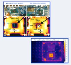
These targeted results show that near-field radiative heat transfer exceeds the far-field radiative heat transfer. This happens when the radiation wavelength is lower than the gap between emitter and receiver. The outcome is an increase in surface area and emissivity where the heat transfer is significant in the far field.
The increase in radiative heat transfer can be even higher when nanostructures are applied in the near field. This process can show enhancements at least 25 times over in radiative heat transfer when the gap between the emitter and receiver is in the near-field range. It is possible the result can be increased even further when the emitter/receiver gap is machined to increase surface area and emissivity, as they are placed in close proximity in the near-field range. This dual technology development in nanostructures and nanogaps between the emitter and receiver enables a wide range of thermal management solutions in heat acquisition, heat transport, and heat rejection. This includes storage in space and terrestrial applications from integrated heat spreaders and heat sinks used in microprocessors to satellite thermal radiators.
Figure 3 shows a darkened copper integrated heat spreader on one side and an untouched side on the other. The darkened side has been machined with a Spirit HE 1040-SHG laser, where, looking at SEM imaging, one can observe the machined area has a 100% surface area increase compared to its normal state. It now has produced fully developed self-organized mound-like structures in comparison to the relatively flat surface before treatment. This provides a range of heat transfer applications, due to copper’s high thermal conductivity, making it an exciting prospect to consistently improve its heat transfer characteristics. For a component like the integrated heat spreader, this process can include converting heat spreader films into “peeling” nano heatsinks or even possibly removing the thermal interface material entirely in advanced packaging production lines. Interfaces in general tend to have very low thermal conductivity compared to the thermal conductivities of the components being assembled, which leaves a great opportunity for microprocessor enhancement as a whole.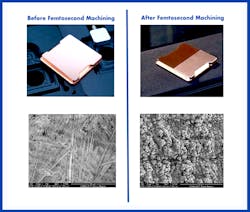
These capabilities and processes have been validated over time and are now being packaged into an ultrafast femtosecond pulse laser unit, the ThermOptical Cooling workstation. This system will allow the creation of new component prototypes and products, while also enhancing the performance of others currently on the market. All of these developments now enable high-throughput manufacturing with femtosecond pulse lasers paired with high-volume manufacturing of thermal management components used in demanding and harsh thermal management systems.
The exponential growth in the number of processors, batteries, and panels for computers, smartphones, IoT devices, and industrial devices combined with the shrinking size of electronic components is providing an opening for femtosecond lasers to meet the rising demand for thermal management solutions. The progress of these lasers over the past 20 years has been remarkable. In the near future, laser surface functionalization via femtosecond lasers may play an important role in meeting this demand for industrial applications and possibly even the consumer market.
REFERENCES
1. See https://bit.ly/3705SWn.
2. See https://bit.ly/3NwxKlF.
3. V. A. Rivas, “Nano machined materials using femtosecond pulse laser technologies to enhance thermal and optical properties for increased surface area to enhance heat dissipation and emissivity and electromagnetic radiation,” U.S. Patent 8238098 (2012).
About the Author
Victor A. Rivas
Founder and CEO, ThermOptical Cooling
Victor A. Rivas is founder and CEO of ThermOptical Cooling (Oro Valley, AZ), where he created its patented laser surface nanomachining technology (U.S. 8,238.098 B1).