Laser cutting system has use in half and shingled solar cell manufacturing

Oct. 5, 2021
The system meets photovoltaics (PV) market demands for boosting module power output and service life by minimizing power losses and providing for an exceptionally high mechanical strength of cut cells.

3D-Micromac AG (Chemnitz, Germany) has introduced its microCELL MCS advanced laser cutting system for half and shingled solar cells. The system meets photovoltaics (PV) market demands for boosting module power output and service life by minimizing power losses and providing for an exceptionally high mechanical strength of cut cells. It enables high throughputs for cutting cell sizes up to M12/G12 into half-cells or shingled cells.

PV module manufacturer Heckert Solar GmbH has purchased two microCELL MCS systems for its plants in Thuringia (LWD Solar GmbH) and Chemnitz.

The microCELL MCS system employs 3D-Micromac’s thermal laser separation (TLS) process, which is ablation-free, for cell separation. The separated cells have up to 30% higher mechanical strength compared to ablative laser processes and enable a lower power degradation over the solar module’s life cycle. TLS has also been shown to achieve a module power gain of at least 2 W.

In standard configuration, the laser system cuts half-cells. Depending on the number of laser sources, the system is able to cut up to sixth-cut cells without decreasing the throughput. It also offers productivity of more than 6000 wafers per hour, and can be integrated with additional laser modules to increase the number of cell cuts. The system works with solar cells with temperature-sensitive coatings or depositions such as heterojunction technology (HJT) cells.
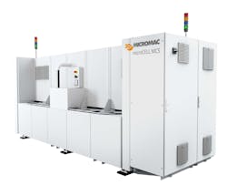
Source: 3D-Micromac press release

About the Author

Industrial Laser Solutions Editors

We edited the content of this article, which was contributed by outside sources, to fit our style and substance requirements. (Editors Note: Industrial Laser Solutions has folded as a brand and is now part of Laser Focus World, effective in 2022.)

Sponsored Recommendations

Monolithic integration of functional structures into micro-optical elements

Dec. 6, 2023
A polymer-only ultraviolet imprint process potentially saves costs, simplifies the process, and increases the reliability of the optical element.

Manufacturing thin films with tailor-made electronic properties

Dec. 5, 2023
Unlock the future of optoelectronics as researchers at Leibniz IPHT in Jena, Germany unveil an innovative technique for precision deposition of thin organic semiconductor films...

Quantitative Microscopy with Deep Learning

Dec. 5, 2023
Explore the untapped potential of deep learning in video microscopy with our cutting-edge software, DeepTrack 2.2. Overcoming the steep learning curve, this innovative application...

Stimulated Brillouin scattering enhances CMOS chip for microwave signal processing

Dec. 5, 2023
University of Sydney Nano Institute researchers are pioneering photonic silicon chips and helping spur growth in Australia’s semiconductor industry.

Voice your opinion!

To join the conversation, and become an exclusive member of Laser Focus World, create an account today!