3D printing improves strain gauge sensor manufacturing
After more than 80 years of use as a sensing element for deformation measurements, the strain gauge has become a matter of course. However, the conventional adhesive-sensor strain gauge is facing new challenges as the industry increasingly demands that the measured values and their digital processing can be reproduced in an automatable process to a far-higher degree. To meet these demands and open up new applications, additive manufacturing technology can be applied to allow for more flexible design, automation, and reproducibility in attaching strain gauges. To appreciate the benefits of additively manufactured strain gauges, a brief review is useful.
The traditional strain gauge and its applications
Strain gauges can be used to record component loads such as forces or moments as changes in shape (strains/compressions) on the surface of these components (see Fig. 1). For this purpose, strain gauges have been continuously revised in recent decades to reduce measurement uncertainties. However, the basic operating principle of the strain gauge has not changed. An electrical conductor undergoes a deformation when a force is applied; both the length and the cross-sectional area of the conductor change, and thus directly its measurable ohmic resistance.
The user will primarily associate the strain gauge with an elaborate procedure required for installing it. This is because bonding requires not only many work steps and corresponding know-how, it also requires experience and the necessary manual sensitivity during installation to transform the strain gauge, supplied on a carrier foil, into a measuring point on the component that delivers accurately measured values. As a matter of principle, the working environment must be kept clean in order to apply a thin adhesive layer free of contamination. For compact force transducers, such as those used in household scales, the hot-melt adhesive process is used. Here, the adhesive-coated strain gauge is pressed onto the measuring point, and the component is cured in an oven.
If the component cannot be placed in an oven due to its size, weight, or temperature sensitivity, the so-called cold bonding method is used. After the bonding area is roughened with sandpaper and degreased, the intended strain gauge position is marked. Marking, positioning of the strain gauge, and subsequent application and uniform distribution of the adhesive are typically performed manually, therefore creating large uncertainties in lateral positioning of the gauge. As the adhesive cures, the strain gauge is pressed against it for approximately one minute. The thickness of the cured adhesive film can vary greatly, which significantly affects how well the sensor responds.
Gluing on a strain gauge is thus problematic in two respects. On the one hand, the manual work steps result in inconsistent quality due to user errors. High quality requirements can be met with a number of aids; however, effort and installation time increase. If the quality of the measuring point is insufficient, the strain gauge must be destructively removed and a new one glued on. On the other hand, the use of qualified personnel is the largest cost fraction in the installation of a strain gauge. For larger quantities, there are no or insignificant cost scaling effects. Therefore, the sensors need to be applied with an automated process.
Added to this is the effort required for the subsequent measurement- and data-transmission chain—things get complicated, especially on rotating components. The usual approach here is to use inductive telemetry systems, which transmit both measurement data and energy via inductive coupling. However, these systems are only suitable for series production to a limited extent since they are prohibitively expensive and not particularly robust. Other alternatives such as surface acoustic wave (SAW) or magnetostrictive sensor technology are only suitable for certain materials or have proven to be susceptible to interference in field use. Thus, they have not yet been able to establish themselves. Progress in the development of low-power industrial solutions for wireless data transmission is opening up new possibilities, which will be exploited here to put sensor technology that does not need external energy sources into practice.
Additive material printing for strain gauge sensors
What opportunities can additive manufacturing offer here? After all, many 3D components can already be printed from different materials. The Fraunhofer Institute for Laser Technology (Fraunhofer ILT) and i4M Technologies (both in Aachen, Germany) have addressed this question and developed a prototype, which is described below.
In conventional strain gauges, the resistive measurement grid is usually laminated between a carrier and cover film. This foil strain gauge is bonded to the component by an adhesive. Strain from the component is transferred to the measuring grid via two intermediate layers (see Fig. 2a). In principle, the measuring grid should be placed as close as possible to the component surface in order to avoid force transmission losses. A variation in bond thickness will be reflected in the force transmission, and the response of the strain gauge measuring point may change. When the strain gauge is applied directly using a printing process (such as inkjet printing), a simpler layer system can be used between the component and the measuring grid (see Fig. 2b). Only one intermediate layer is required, which combines the function of force transmission and electrical insulation between the component and the measuring grid.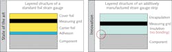
How the strain gauge is created using 3D printing technology
In the additive manufacturing approach shown here, three functional layers—an insulation layer, the metallic measuring grid, and a cover or encapsulation layer—are printed one after the other and then each is functionalized. The functions of the carrier film and adhesive in conventional strain gauges are taken over by a single insulation layer. This way, the measuring grid can principally be positioned closer to the component surface, thus promising improved strain transfer to the sensory measuring grid.
Which processes are suitable for the layer buildup? The processes should be digital, save resources, work inline, have already proven they are robust enough on an industrial manufacturing scale, and above all reduce manufacturing costs per sensor.
Before an additively manufactured strain gauge can be applied to a component, the component surface can be cleaned of interfering substances such as rust, residual lubricants from prior process steps, or oxide layers using laser radiation. This step can also be adapted to roughen the surface: Microscopically small areas are selectively ablated, remelted, or modified using pulsed laser radiation to increase the adhesion of the layers applied later.
Dispensers and inkjet printers can deposit the materials at the point of measurement selectively. Post-treatment is carried out with efficient light sources (laser or LED), which quickly couple the necessary energy into the printed layers without unnecessarily heating the component.
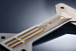
A hybrid polymer, such as ORMOCER invented by the Fraunhofer Institute for Silicate Research (Fraunhofer ISC; Würzburg, Germany), can be used as an electrical insulation material. It is available in an uncrosslinked form as a viscous material and can be photoinitiated (that is, crosslinked by means of light irradiation). The material can be applied selectively by means of dispensing, so the hybrid polymer is only applied to the required areas (see Fig. 3). A CNC control system guides the dispenser and ensures precise positioning. A light source then cures the layer in a few seconds. Below is a comparison of the standard foil-based and additively manufactured strain gauge layer construction steps.
Layer construction of a standard foil-based strain gauge:
- Cover foil
- Measuring grid
- Carrier foil
- Adhesive
- Component
Layer construction of an additively manufactured strain gauge:
- Encapsulation
- Measuring grid
- Insulation (no adhesive)
- Component
A digitally printed strain gauge post-processed by a laser basically makes it possible to reach constant quality independent of manual processes and at attractive costs in series production. The approach has particular strengths in highly flexible small-batch production, since customized designs can be created without needing to retool. However, all the challenges of process development have not yet been solved. For example, to date there are only limited metallic inks and insulation materials that enable material-matched temperature compensation or defined force transmission, or that have been developed for laser functionalization processes. For this reason, Fraunhofer ILT is working together with research partners and industrial users on continuous further development.
From the measuring point to the smart sensor
However, the strain gauge as a sensor alone is not enough, as the measurement data of smart components must be digitized, transmitted, and analyzed. Measurement data now becomes “smart data” (economically usable data), which can mean remaining service life, automated maintenance plans, optimized control strategies, and more, all of which form the basis for concepts such as predictive maintenance. In order to measure component loads precisely, strain gauge-based measuring points must be applied in the force flow. However, there is not much space, especially in modern machines. Furthermore, the price pressure for such solutions is high, especially when quantities increase and a solution ready for series production is required.
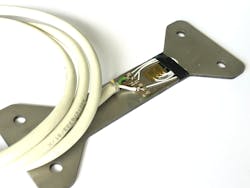
A highly integrated low-power radio telemetry was developed to transmit data from the additively manufactured sensor and applied to a component together with the strain gauge (see Fig. 4). The latest commercially available hardware is used, and power efficiency is pushed to a maximum employing an optimized firmware:
- Ultra-low-power system-on-chip consisting of a Cortex M4 MCU and 2.4 GHz radio modem
- Analog measurement front-end with 24-bit ADC, integrated signal amplifier, and reference voltage source
- Additional six DOF MEMS sensors (accelerometer, gyrometer), as well as temperature sensors
- Lithium-ion battery or lithium primary cell with suitable charging electronics and protection circuits
A specially developed protocol is used for data transmission in the 2.4 GHz band, which enables higher data rates with low latencies compared to Bluetooth and other industrial protocols. The maximum possible sampling rate is 19.2 kHz, which can also be streamed on-air. However, the power requirements and, thus, the battery runtimes are directly dependent on the selected sampling rate. Since the strain gauge measuring bridge has the highest power requirement, it is operated in pulsed mode, but this is only possible up to certain sampling rates. In addition, all components can be operated in low-power sleep modes for significantly shorter periods at higher sampling rates. While—depending on the battery—the continuous runtime at 19.2 kHz is hours up to days, years of runtime are possible in discontinuous operation and at lower sampling rates.
Thanks to this solution, high-performance, energy-autonomous sensors can be manufactured under tight installation space restrictions for highly available components. This sensor technology has already been successfully used in various technical systems ranging from gear wheels and roller bearings rotating in warm oil to railroad systems or wind turbines under strong electrical interference fields and severe vibrations. The computational capabilities available on the MCUs also allow edge-analytics (for example, FFTs) to be conducted on the sensor. These smart sensors can achieve a strong reduction in the amount of data transmitted and, thus, a further energy efficiency gain through edge computing. Furthermore, online algorithms in the sensor make it possible to increase the quality of the measured values obtained—for example, by sensor fusion or suitable filters.
However, one limitation of the telemetry solution shown here remains: battery operation. Years of battery life are feasible, but they are finite—this is why energy harvesting approaches are now coming into play. At i4M Technologies, promising approaches based on temperature and RF harvesting have already been successfully investigated.
About the Author

Matthias Rehberger
Research Associate, Thin Film Processing Group at Fraunhofer ILT
Matthias Rehberger, M.Sc., is a research associate in the Thin Film Processing group at the Fraunhofer Institute for Laser Technology (Fraunhofer ILT; Aachen, Germany).

Martin-Christopher Noll
Managing Director, i4M technologies GmbH
Dipl.-Ing. Martin-Christopher Noll is the managing director of i4M technologies GmbH (Aachen, Germany).
Christian Vedder
Head, Thin Film Processing Group at Fraunhofer ILT
Dr. Christian Vedder heads the Thin Film Processing Group at the Fraunhofer Institute for Laser Technology (Fraunhofer ILT; Aachen, Germany).