Hamamatsu Photonics delivers highest-to-date pulsed laser power capability
Hamamatsu Photonics (Hamamatsu, Japan) has developed a liquid-crystal spatial light modulator (SLM) that is said to offer the world’s highest pulsed laser power capability up to 400 GW/cm2. This new SLM for high-power industrial pulsed laser systems will contribute to achieving high-throughput, high-precision laser processing and processing resistant materials such as lightweight and high-strength carbon fiber-reinforced plastics (CFRPs).
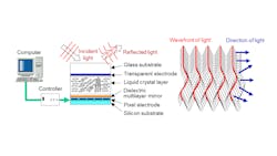
A SLM is an optical device that utilizes liquid crystals to control the wavefront of incident light such as lasers to freely modulate the wavefront shape of the reflected light. A liquid-crystal layer is sandwiched between a silicon substrate with pixel electrodes and a glass substrate with transparent electrodes. The path length of the incident light is varied by controlling the inclination of each liquid crystal according to the signal sent to the pixel electrodes from a PC, and the reflected light is in this way modulated, allowing the laser irradiation pattern to be controlled—for example, to branch the incident light or correct its distortion.Currently, pulsed lasers emit light pulses that allow high-precision laser machining with minimal heat damage. Because their precision is higher than conventional mechanical machining, pulsed laser machining is becoming widely used for processing resistant materials such as CFRP and low dielectric constant (low-k) materials that prevent a drop in operating speed in semiconductor integrated circuits. However, several issues remain, such as the machining speed and processing throughput.
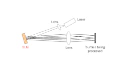
Incorporating a SLM into an industrial pulsed laser system improves the processing throughput compared to laser machining that uses only a single focused beam, but so far the output power required for machining has been inadequate. Due to this, industrial pulsed lasers with higher output power are becoming available on the market, which creates an increasing demand for a SLM to have even higher resistance to laser power.
Hamamatsu Photonics has already developed and produced optical wavefront control devices with high resistance to light, mainly for laser marking applications for engraving characters and QR codes on objects moving at high speed on production lines. By reviewing the thin-film design for dielectric multilayer mirrors that reflect the incident laser, and by redesigning the pixel electrode circuit, Hamamatsu increased the light resistance up to 400 GW/cm2, which is more than 10X higher than the company’s previous products.Using this newly developed SLM with a higher power pulsed laser allows simultaneous irradiation of a target sample with multi-beams, while maintaining adequate output power. As a result, this achieves high-throughput and high-precision laser processing of processing-resistant materials such as CFRP used for aircraft and transportation equipment and low-k materials used for 5th generation mobile communication systems (5G).
For further information, please contact [email protected] or visit hamamatsu.com.


