Ultrashort-pulse laser applications advance
ERIC MOTTAY
The manufacturing industry is facing two difficult challenges across all applications. The complexity of modern devices is continuously increasing: With higher resolution and components density, feature sizes are now reaching dimensions incompatible with more-traditional processing technologies. In addition, high-resolution displays, new medical implants, or high-density semiconductors increasingly make use of different and complex materials, such as glass, organic polymers, copper, or ceramics. These materials are very difficult to process, and even state-of-the-art lasers are now reaching their limits.
Over the past decade, ultrashort-pulse (USP) lasers have enabled the industry to keep pace with the need for ever-higher resolution and smaller feature sizes, and the increased complexity of modern devices. These lasers concentrate the output energy in a very short duration, typically in the femtosecond to low picosecond regime, and deliver an extremely high optical intensity. The radically different nature of the laser-matter interaction process provides two key advantages, well matched to industrial demands.
How USP lasers compare
In contrast with traditional regimes, the USP duration and the very high intensity on the target lead to a complete ionization of the irradiated volume by nonlinear effects. Since the pulse duration is below the heat diffusion time, the material is ejected before any heat diffusion or thermal damage can take place, leading to a high processing quality. Moreover, because of the very high optical intensity, virtually any material can be processed with USP lasers, solving previously intractable manufacturing challenges. These lasers are now a strategic part of important industrial and medical applications, as they treat cataracts, manufacture medical implants, enable innovation in modern smartphones, and can even be applied to microwelding of glass and ceramics.
Yet, a new frontier remains open to USP laser applications: Because of the precise, nonthermal nature of the ablation process, the quantity of matter removed per laser pulse is relatively small, sometimes limiting the industrial productivity or throughput. The ablation efficiency, expressing the quantity of matter removed per minute and watt of laser power, is typically on the order of 0.5 mm3/m/W.
Increasing the throughput of USP processes would open up a range of new applications and markets. As an example, using USP lasers for surface modification or texturing can impart a material with extremely useful functions. Hydrophilicity or hydrophobicity can be used for self-cleaning surfaces, deep black marking of metal is extremely interesting for esthetics purposes, antibacterial properties could be conferred to large surfaces, and reduced friction increases fuel efficiencies. The technical feasibility of all these processes has been abundantly demonstrated and some of them are used in industrial manufacturing. Marking and texturing are applied to high-end, luxury watches or advanced consumer electronic devices.
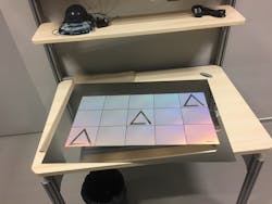
However, specific markets, such as aeronautics or the automotive industry, often require precision processing over a large area (FIGURE 1). The development of surface texturing applications is still limited by the time required to treat a large surface. Increasing the ablation efficiency and industrial throughput of USP laser processing is a key requirement to fulfill the needs of these new domains.
Since the ablation efficiency is expressed in units per watt of laser power, the first and most straightforward approach is to increase the average power of USP lasers. To this end, the USP laser industry has been following its own Moore’s law for the past 20 years, with a doubling of the laser power every two or three years.
Further USP laser developments
The first generation of USP lasers, introduced in the early 2000s, had an average power of 1 W—today, most industrial applications lie in the 10–100 W range. Industrial lasers with a 100 W output power are commercially available from several manufacturers, most operating with moderate pulse energy (typically <300 µJ) and high repetition rate (up to several megahertz). They are used in high-throughput manufacturing applications, such as glass cutting or drilling for smartphone displays.
In addition, several European research projects aim at the development of kilowatt-class industrial femtosecond lasers. However, the average power of the laser alone is not sufficient to guarantee industrial productivity. Although the nature of the laser-matter interaction is virtually athermal in the sub-picosecond domain, heat accumulation occurs when operating the laser at high repetition rates, leading to detrimental thermal effects. The question is therefore how to make the best use of the high average power available while maintaining a high processing quality.
Achieving a high average power is possible either by increasing the pulse energy, or by increasing the repetition rate—that is, the number of pulses emitted per second. This gives rise to two main strategies to achieve high-throughput, high-quality laser microprocessing.
Increasing the pulse energy has the advantage of keeping the repetition rate low and therefore manageable with current scanning techniques. However, most processes require only a moderate energy, on the order of a 100 µJ, to achieve an optimum quality and efficiency. Splitting the laser beam in multiple sub-beams using, for instance, diffractive optical elements allows efficient use of these higher pulse energies.
Increasing the repetition rate allows keeping a pulse energy compatible with the best process efficiency and quality. However, the repetition rate can reach several megahertz, and heat accumulation can lead to important thermal effects. High-speed beam scanning becomes essential and new scanner technologies, such as polygon scanners, are being actively developed.
High-throughput femtosecond laser processing therefore requires a multidisciplinary approach, involving high-power lasers, innovative beam engineering, and application development. Within the framework of the Horizon 2020 research program of the European Union, several multipartner research projects address high-productivity manufacturing:
The TRESCLEAN project (tresclean.eu) aims at developing high-throughput laser-based texturing for fluid-repellent and antibacterial metal surfaces (FIGURE 2). The end goal is to produce self-cleaning and aseptic machine parts for the food industry and home appliances (for example, dishwashers).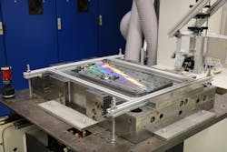
The MULTIFLEX project (multiflex-project.eu) investigates the coupling of acousto-optic and diffractive optical development to achieve large area surface texturing of metals with kilowatt industrial USP lasers. Applications include structuring and embossing of mold and tools for the automotive and printing industries.
The MULTIPOINT project (multipoint-project.eu) concentrates on high-throughput microdrilling of large titanium panels used in the fabrication of large hybrid laminar flow control (HLFC) structures in the aerospace industry.
Whether ultimately applied in the food, printing or aerospace industries, these three projects illustrate the strong drive across all sectors to achieve high precision laser micro-processing on a large scale.
In addition, the field is ready for new, innovative, and disruptive technologies. The uses of spatially shaped beams, such as nondiffractive Bessel beams, are a key to high-speed, high-quality glass cutting. Another approach, using bursts of pulses at a gigahertz repetition rate is showing promising results. Laser conferences across the world emphasize the amount of cutting-edge research now being carried out in laboratories, technology centers, and industrial companies. This creative and innovative approach, coupled with the near availability of industrial kilowatt-class femtosecond lasers, is the key to future high-throughput applications of USP lasers.
ERIC MOTTAY ([email protected]) is the president and CEO of Amplitude Laser, Pessac, France (amplitude-laser.com); he is also a recurrent contributor to Industrial Laser Solutions.