CO lasers benefit via drilling and wafer debonding
The carbon monoxide (CO) laser has been known for almost as long as the widely used carbon dioxide (CO2) laser, but has only recently gained significant interest for industrial applications. This article highlights the potential for CO lasers to play an important role in microelectronics manufacturing, specifically for drilling ≤40 µm microvias in PCB material and in the developing field of silicon debonding.
CO laser background
CO lasers emit in the 5–6 µm spectral range, which offers two important advantages for some applications when compared to the far-infrared (10.6 µm) output of the CO2 laser. Many metals, films, polymers, PCB dielectrics, ceramics, and composites exhibit significantly different absorption at the shorter wavelength. Given a higher absorption at the shorter wavelength, material can be processed more efficiently using lower laser power, and with a smaller heat-affected zone (HAZ). On the other hand, when the transmission is higher at the shorter wavelength, the light penetrates farther into the material, which can also be advantageous.
Another advantage of shorter wavelengths is that they can be focused to smaller spot sizes due to reduced diffraction, which scales linearly with wavelength. For example, in a standard configuration, the minimum spot size achieved in practice for CO2 lasers in industrial applications is 70–80 µm, whereas the CO laser can achieve practical spot sizes in the 30–40 µm range. This means that at a given power, the CO laser spot can have a power density (fluence) that is 4X higher than that of the CO2 laser. When combined with stronger absorption at 5 µm in some materials, this enables these materials to be processed with a CO laser at significantly lower powers.
However, despite these advantages, two key operational barriers have impeded wide-scale commercialization of CO laser technology. First, they previously delivered high operational efficiency only at cryogenic temperatures, and second, sealed devices suffered from rapid power degradation. Coherent (Santa Clara, CA) engineers solved these issues and in 2015, the company introduced a series of industrial sealed CO lasers that operate efficiently at room temperature, with operational lifetimes comparable to CO2 lasers.
The most promising initial applications for CO lasers have been in glass scribing (cutting) and for a glass separation step that sometimes follows filamentation (for example, SmartCleave) glass cutting. CO lasers have already demonstrated success in ceramic scribing, cutting, and drilling.
PCB drilling
Via drilling is an important laser application in which CO lasers now offer distinct advantages. Vias are small holes drilled in electronic printed circuit boards (PCBs) to enable electrical connections to be made between layers (by plating the vias with metal). Just as with integrated circuits themselves, there is an ongoing drive to increase the density of the circuits on PCBs, which in turn creates a need for smaller vias.
Traditionally, vias were produced using mechanical drilling, and this method is still in widespread use for PCBs with lower circuit density. However, in the mid-1990s, CO2 laser via-drilling systems were introduced to enable volume production of PCBs with via diameters of ≤100 µm, which is difficult to achieve with mechanical drilling systems. Currently, CO2 laser-based via drilling systems are routinely utilized to produce via hole diameters between 50 and 100 µm.
Now, the drive for even-higher packaging density is trending towards via diameters between 20 and 40 µm. The previously mentioned ability to focus the CO laser to a smaller spot, combined with the relatively high available output power, makes this technology a good candidate for this application.
Coherent has been conducting via drilling tests to determine the viability and practicality of the CO laser for this application. FIGURE 1 shows cross-sections of the latest via drilling results in FR4, which is a commonly used PCB material. The FR4 dielectric layer consists of a 25-µm-thick fiberglass/epoxy composite with 4-µm-diameter woven fiber. The outer copper layer had a brown oxide surface treatment to increase laser absorption, thereby decreasing the power required to drill through the copper layer. This is a standard surface treatment used in CO2 via drilling systems. Material samples with either a 9 or 3 µm copper outer layer were laser-drilled. The detailed pulse format used to drill the vias is provided in the figure caption. As shown, clean, ≤30-µm-diameter vias with minimal taper and no damage to inner-layer copper were achieved in both materials.
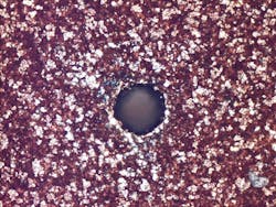
FIGURE 2 shows a top-down view of a 40 µm via with very clean walls and a clean bottom copper layer with essentially no glass residue. The 5 µm wavelength of the CO laser enables via diameters as small as 25 µm. The results presented here are from a CO laser with ~1 kW peak power at the workpiece. Testing with a higher-power CO laser is already in process, which will deliver both improved drilling speed and superior process control. This will enable production of extremely uniform vias in a wide range of materials, including different thicknesses of the top copper layer.
Silicon wafer debonding
The next step in increased circuit density beyond traditional PCBs is the use of so-called “advanced packaging” technologies, where multiple integrated circuits are encapsulated in a single package to form a functional unit that contains logic, memory, and/or sensor functions.
Integration of semiconductor devices into ever-thinner packages often requires handling of components that have been thinned to dimensions below 100 µm thickness. To facilitate high-yield thinning, handling, and transfer of such devices, temporary bonding to a thicker substrate is usually employed.
Both glass and silicon have been used for this temporary handling. While glass handlers have reached a high level of industry adoption and technical maturity, interest in silicon as a temporary carrier is remaining strong as the requirements on packaging processes and materials have become more stringent. Specifically, the physical properties of silicon (higher thermal conductivity, matched thermal expansion, reduced warpage, and broad compatibility with existing semiconductor equipment) offer process technology advantages that are driving efforts to continue the use of silicon for temporary wafer handling.
One key barrier to broader adoption of silicon for temporary wafer bonding has been the lack of practical and cost-effective optical debonding technology. Thermal sliding and mechanical peeling approaches are less attractive than optical debonding due to limitations imposed by the thermal and mechanical stresses associated with these methods.1
Unfortunately, silicon is opaque at the UV laser wavelengths employed in commercial glass debonding equipment, and no laser-based debonding technologies are currently commercially available at wavelengths compatible with silicon’s transparency window. CO2 lasers, the industry’s workhorse for nonmetal materials processing, also falls into an incompatible wavelength range. Nevertheless, a room-temperature laser-based wafer debonding technology is an attractive notion that would be an important and practical enabler for wider use of silicon wafers as temporary handlers.
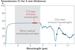
FIGURE 3 illustrates that silicon is transparent at the CO output wavelength for typical substrate thicknesses, while the CO2 laser wavelengths fall outside the window of transparency. Moreover, CO lasers are now available in a range of configurations and power ranges that allow processes to be developed with output formats from nanosecond pulses to continuous-wave, and power levels up to 400 W. This makes them well suited to processing various release layer and adhesive formulations, and compatible with both spin-coated and vapor phase-deposited materials. From a tool integration perspective, CO lasers share a great deal of interface commonality with the more-mature CO2 laser technology base, facilitating a relatively low-risk development path to a production-worthy debonding process.
Conclusion
The mid-infrared output of the CO laser provides an industrial tool in a spectral range that has previously been largely inaccessible. The potential applications for this technology are just now being explored and developed. In addition to various glass and ceramic processing tasks, via drilling and wafer debonding are two other applications that show tremendous potential.
ACKNOWLEDGEMENT
SmartCleave is a trademark of Coherent.
REFERENCES
1. B. Dang et al., “Feasibility study of Si handler debonding by laser release,” 2016 IEEE 66th Electronic Components and Technology Conference (ECTC), 1671–1677 (2016); doi:10.1109/ectc.2016.288.
2. C. Shi, M. Ermold, G. Oulundsen, and L. Newman, “CO2 and CO laser comparison of glass and ceramic processing,” Proc. SPIE, 10911, 109110M (Feb. 27, 2019).
About the Author
Peter Rosenthal
Peter Rosenthal is manager, technology and product development at Coherent Corp.
Dirk Müller
Dirk Müller is director of global account management at Coherent Corp.
George Oulundsen
George Oulundsen is senior director and general manager at Coherent Corp.


