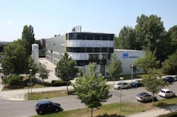
Jenoptik responds to demand for high-power laser diodes
Jenoptik (Jena, Germany) is investing in modern production equipment at its location in the Adlershof Technology Park in Berlin, Germany to ensure long-term competitiveness in a photonic core business. New machines and systems speed up order processing for the production of high-power laser diodes at this location. The company is one of a few independent specialists in the complete processing and technology chain, from laser semiconductor material to customer-specific application solutions. The expansion of production and clean rooms will lead to new employees, increasing to 75 by the end of 2018.
A new stepper is used to manufacture laser diodes, increasing production capacity, yield rate, and quality, resulting in reduced delivery times. There has been an investment in new equipment for facet coating. In the medium-term, investment in the low double-digit million euro range is planned in all three production areas of facet coating, wafer processing, and epitaxy.
Semiconductor bars manufactured by Jenoptik are increasingly used in the healthcare and life science sectors, for advanced manufacturing technologies as well as for cutting-edge sensor systems, which advance trends in the automotive industry such as autonomous driving.
In 2002, the Jenoptik Diode Lab at the Berlin location was established as a spinoff from the Ferdinand Braun Institute, Leibniz Institute for High Frequency Technology (FBH). In 2006, Jenoptik opened the high-tech production of semiconductor lasers. The extension that followed in 2012 was one of the Jenoptik Group's largest single investments, costing around 10 million euros. The 2900 square meters, 950 square meters of which are clean rooms, is available for epitaxy, wafer processing, and facet coating, providing a complete production line for manufacturing semiconductor lasers.
In the typical semiconductor manufacturing process, wafers are structured and processed into laser bars. The laser bars produced in Berlin are supplied to customers worldwide and are processed into high-power laser diodes, and at Jenoptik in Jena they are integrated into other laser systems.
For more information, please visit www.jenoptik.com.
