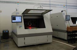
NSI Laser opens micromachining applications laboratory
Laser micromachining specialist NSI Laser (Fremont, CA) is opening an applications laboratory at its Fremont facility in response to the electronics industry moving towards high-density interconnect (HDI) and finer-geometry PCBs.
As new materials enter this miniaturization challenge, the demand for new and advanced laser micromachining processes increases. The new App Lab is equipped with the company's dual-head laser systems and features analytical capabilities such as 3D imaging for real-time sample process evaluation.
The App Lab will be managed by Dr. Yung Kuo as its senior laser applications engineer, who brings over 25 years of practical laser micromachining experience and process development.
NSI Laser's systems perform a variety of processes such as etching, drilling, skiving, and routing, and can handle most mixes and volumes.
For more information, please contact [email protected] or visit www.nsi-usa.com.

