Selective soft laser soldering
Daventry, U.K. – Using a laser for selective soldering operations allows the thermal energy required to be applied directly to the joint with no physical contact. In addition, the ability to focus the laser energy to a concise point means that the heat input area is localized and highly accurate. The narrow beam profile of the laser also enables soldering operations to be carried out in hard-to-reach areas, offering a significant advantage over conventional methods.
Traditional soldering technologies can pose problems when applied to delicate or temperature-sensitive parts. A soldering iron requires direct mechanical contact and this can bring with it the risk of contamination in the joint. The size of the iron can make it difficult to gain easy access and there is little in the way of temperature control using this method.
Reflow soldering techniques are not always appropriate due to the presence of adjacent parts or access to the specific joint area, and hot air principles pose a potential heat risk to surrounding components. Using the laser process, solder can be presented by an automated solder wire feed system or in the form of solder paste or pre-tinned contacts.
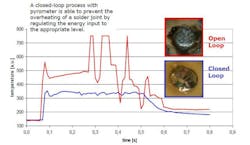
Process control in laser soldering is achieved using a pyrometer, which also serves as a reliable quality monitor. This non-contact method of measuring the temperature of the soldering process enables a closed loop system to be created, balancing temperature (Fig. 1) and laser power to provide consistent and predictable results.
Diode lasers in solar cell production
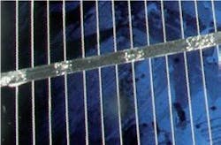
In addition to the many advantages that diode lasers bring to the electronic manufacturing sector, they also have all of the properties necessary for laser soldering and contacting on thin film solar cells. The solder joints, which can be achieved by using cw diode lasers, cover several square millimetres (Fig. 2). This non-contact technology together with the accurate and highly localized thermal input limits the potential for thermal stress in the cell. Usually Si solar cells are interconnected to strings, which in turn are laminated into the modules. This process requires subsequent handling with additional equipment for these long and fragile strings.
Using a laser and galvo-scanner combination, however, the string handling can be completely eliminated by soldering directly through the laminate layers without the need to move the optics or the cell. The typical composition for these modules is glass, polymerized ethylene vinyl acetate (EVA), tinned ribbons, solar cell, tinned ribbons and a transparent PVF (polyvinyl fluoride) back sheet. The front and rear sides of the PV module are transparent to laser radiation. Soldering can therefore be done either before or after lamination.
With regard to peel force and contact resistance, the quality of the laser soldered joints exceeds that of other contacting technologies. The peel force is higher by a factor of 3, whereas the thermal resistance is only about 14% of the contact solder joint.
DILAS, the diode laser company, is focused on delivering the most innovative technologies and advanced product solutions for the industrial market. Diode-based laser soldering is one example.
For further information, please contact Dave MacLellan, sales manager, Micro Division, Rofin-Baasel UK Limited, [email protected].


