Laser micromachining of polymer nanocomposites and sol-gel thin films for flexible and printable nanomaterials
By Rabindra N. Das, Frank D. Egitto, Timothy E. Antesberger, Francesco Marconi, How Lin, John M. Lauffer, and Voya R. Markovich, Endicott Interconnect Technologies Inc.
This article discusses laser processing of polymer nanocomposites and sol-gel thin films, highlighting recent developments in vertical multilayer embedded capacitors. A variety of flexible, transparent nanocomposite thin films ranging from 2-microns to 25-microns thick were processed on copper, ITO, or organic substrates by large area (330mm x 470mm or 495mm x 610mm) liquid coating processes. A frequency-tripled Nd:YAG laser operating at a wavelength of 355nm was used for the micromachining study. The micromachining was used to generate arrays of variable-thickness capacitors from the nanocomposites. The resultant thickness of the capacitors depended on the number of laser pulses applied. Laser micromachining was also used to make long, deep multiple channels from a capacitance layer. Spacings between two channels act as individual vertical capacitors, and parallel connection eventually produces vertical multilayer capacitors. Optical photographs and SEM micrographs were used to view spacings/channels in the coatings. In the case of sol-gel thin films, micromachining resulted in various surface morphologies. It can make a "wavy" random 3D structure, or an array of regular 3D patterns (spirals/lines) depending on laser fluence. Altogether, this is a new direction for the development of multi-functional nanomaterials.
Increasing volume, complexity, and density of next generation electronic packaging products
Material formulation, structuring, and modification are keys to increasing the unit volume complexity and density of next generation electronic packaging products. Laser processing is finding an increasing number of applications in the fabrication of these advanced microelectronic devices. This is due, in part, to the ability to achieve highly localized treatment of materials with a spatial resolution of tens of microns. In addition, the process is data-driven, that is, patterns can be generated without the need for masking materials. Laser processing parameters, such as fluence and wavelength, can be adjusted to suit a specific application, such as micromachining (ablation) or annealing. Laser micromachining has been used for years as a means of microvia formation for electrical interconnection in microelectronic devices. This method can be utilized to generate other new structures in nanocomposite materials without altering the dielectric properties of the nanocomposites. Conversely, laser annealing improves particle contact, or sintering, or crystalinity of the thin film, resulting in variation of dielectric properties. As such, laser annealing can be used to control crystallinity, phase content, morphology, and dielectric properties of materials.
Laser annealing also heals defects, and is a good approach for repair of passives. In the present investigation, laser-materials interactions have been investigated for a variety of nanostructured films including zinc oxide, titanium oxide, silicon dioxide, barium titante, and iron oxide. This article addresses the utilization of polymer nanocomposites as it relates to printable and flexible technology for electronic packaging and system integration. Printable technologies such as screen-printing, ink-jet printing, and microcontact printing provide a fully additive, non-contacting deposition method that is suitable for flexible packages for a variety of applications. A variety of structures have been generated in polymer nanocomposites, nanoparticle films, and sol-gel thin films using a computer-controlled laser system. Specifically, micromachining technology has been used to produce both variable-thickness and discrete capacitors from a single sheet (layer) of capacitor material, such that both types of structures can be integrated into the same layer. In addition, the laser micromachining technology has been extended to design and develop new vertical multilayer embedded capacitors for high speed applications. High speed packages require thick dielectrics. Calculations show that multilayer vertical capacitors can be better than thick capacitors formed from a single layer. Typically, multilayer embedded capacitors are fabricated by repeated lamination of resin-coated copper, or pre-preg with a capacitor core. This is a time consuming, lengthy process. As an alternative, we have deposited a single, thick capacitance layer, and subsequent laser micromachining has been used to form multiple parallel channels of a controlled depth. Metal deposition in the channels results in a multilayer embedded capacitor structure. Laser micromaching can also provide various complex patterns such as 3D spiral channels within a dielectric or magnetically active nanocomposite, subsequently filled with conducting materials to form inductors. This technique can be used to prepare inductors and capacitors in the same layer of nanocomposite material. Hence, the technique can be used to generate multifunctional structures for tunable device applications.
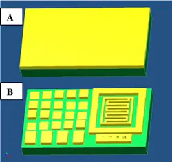
Figure 1 shows a schematic representation of a laser micromachined substrate. As can be seen, part of a capacitance layer deposited on a substrate can be converted to arrays of variable thickness, vertical multilayers and discrete capacitors by laser micromachining.
FIGURE 1. Schematic presentations of (A) the capacitance layer and (B) laser micromachining, top view showing a library (arrays) of discrete and variable-thickness capacitors (prior to deposition of metal for upper electrode).
Sol-gel thin films were prepared by mixing appropriate amount of metal alkoxides in solvents.
The nanocomposite and sol-gel thin film were micromachined under a variety of conditions to form various surface morphologies and capacitor arrays.
Nanocomposites in printing technology
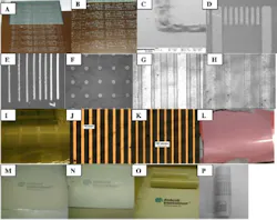
Printable nanocomposites have potential applications at all levels of microelectronics (see Figure 2A-E). This article examines the use of nanocomposites in the area of printing technology. Printing processes have several advantages, such as selective deposition, repair and re-print capability. However, printed features with desired properties, thickness, and tolerance present significant challenges. Embedded resistors, capacitors, and conducting circuit lines can use ink-jet or screen printing for different applications. Figure 2 shows a series of printable and flexible nanomaterials. Ink-jet printing is best performed with inks having low viscosity, in the range of 7-10 cp. Low viscosity helps to generate nano to submicron thin structure.
Screen printing is best performed with higher viscosity pastes (100,000-150,000 cp), and generates 10-25 micron thick features. Figures 2A-2E represent features made with screen printing. It can be seen that screen print can produce line features in the range of 100 microns. Figures 2F-H represent features made with ink-jet printing, showing minimum line feature size in the range of 75-100 microns, and ~50 micron dot patterns. Space between two ink-jet printed lines can be reduced to 50 microns. Figure 2P represents ink-jet printing on flexible substrates.
Several classes of flexible nanomaterials can be used to form high-performance flexible packaging. Transparent electronic circuits are expected to serve as the basis for new optoelectronic devices. Transparent conductive thin films such as indium tin oxide (ITO) and conducting polymers are widely used for liquid crystal displays, touch sensors, solar cells, and flexible displays. In the present work, development of a variety of transparent flexible nanocomposite thin films is discussed.
Figures 2I-2K represent flexible, transparent piezoelectric nanocomposite thin films deposited on flexible substrates. It is possible to make fine circuitry (25-50 microns lines) in flexible piezoelectric nanocomposites. The use of high dielectric constant barium titanate polymer nanocomposite thin film for the gate insulator has several potential advantages, including high capacitance to increase the drain current while operating at lower gate potentials. Thin film barium titanate nanocomposites are nearly transparent. Transparency reduces with increasing thickness of nanocomposites. Figure 2L shows barium titanate nanocomposites deposited on a Cu substrate. The color of the underlying copper substrate is more apparent for the thinner nanocomposite films. Films that are two to three microns thick are nearly transparent, and the color of the copper substrate is clearly visible. Figures 2M-O show large-area, thin, flexible transparent capacitors having 77% (K)-86% (J) filler loading deposited on a flexible ITO substrate. Capacitors can be rolled without damaging the structure. For conventional composites, rolling or bending will cause structural damage such as cracking. The remarkably increased flexibility of the nanocomposite is due to uniform mixing of nanoparticles in the polymer matrix, resulting in an improved polymer-ceramic interface. Integration of this flexible and transparent capacitance layer into a flexible structure could be useful for developing high–performance, multilayer, flexible electronics, such as roll-up displays, e-papers, transparent thin-film transistors (TTFT) and keyboards.
FIGURE 2. Various printable and flexible nanomaterials (A)-(B) screen print with printed area (152mm x 305mm), (C) enlarged screen print, (D) screen printed resistors, (E) screen printed zinc oxide nanocomposite, (F)-(H) ink-jet print, (I)-(K) flexible piezoelectric nanocomposites with fine circuits, (I) flexible capacitors on Cu substrate, (M)-(O) transparent flexible/rollable capacitors deposited on ITO based substrate, and (P) ink-jet printing on flexible plastics.
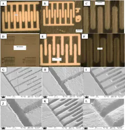
Figure 3 shows top views of laser micromachined channels for vertical multilayer embedded capacitors.
FIGURE 3. Optical photographs and SEM micrographs of laser micromachined channels for vertical multilayer embedded capacitors.
It is possible to make a wide variety of channels with different spacings. The spacing between two channels determines the capacitor thickness, and therefore, affects the capacitance value. For a given channel depth and dielectric constant, the smaller the spacing, the higher the capacitance. The desired spacing between two channels can be achieved by controlling the laser micromachining parameters. In the present process, we can easily make spacings from about 5 microns to about 50 microns. Figure 3 shows a variety of samples with average spacings of 5 microns, 10 microns, and 25 microns, as typical representative examples. It is also possible to control the channel width by controlling the laser beam width. Channel widths of 10 microns to 35 microns are demonstrated here. The image of a 5-micron spacing is shown in top view in Figures 3A and F. BaTiO3 epoxy nanocomposites were used to fabricate vertical multilayer embedded capacitors. High temperature/pressure lamination was used to embed capacitor dielectric in multilayer printed circuit boards. The capacitor fabrication is based on a sequential build-up technology. First, channels are micromachined into the embedded capacitor material. After patterning of the channel, the conducting material (Cu/Ag/Au) can be deposited within the channel. Conducting materials can be directly deposited either by sputtering or plating processes.
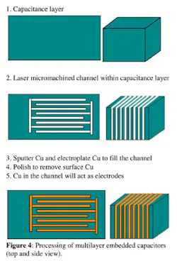
BaTiO3-epoxy nanocomposite thin films with vertical multilayer embedded capacitors can be used as the base substrate for subsequent build-up processing. Figure 4 shows a schematic process flow for making multilayer vertical embedded capacitors from a capacitor base substrate.
FIGURE 4. Processing of multilayer embedded capacitors (top and side view).
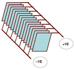
The embedded capacitor can also act as a subcomposite and can be laminated with other sub-composites for making high layer count boards with embedded capacitors. Capacitance values are defined by the feature size, spacing, and dielectric constant of the polymerceramic compositions. Multilayer embedded capacitors are shown schematically in Figure 5.
FIGURE 5. Multilayer embedded capacitors (MLECs). Capacitance layer is vertically sliced by laser micromachining.
As the spacing between the micromachined channels is decreased, the corresponding capacitance increases. In other words, micromachining can generate multilayer capacitors with variable capacitance density. Epoxy/BaTiO3 nanocomposite layers with a dielectric constant around 30 have been fabricated. For a given volume of capacitor material, a theoretical capacitance calculation was made considering variable channel widths and spacings. For comparison, calculations were also made for a "normal" capacitor, that is, a horizontal capacitor having a single pair of electrodes.
Decreasing the spacing and channel width can accommodate more capacitors per unit volume and results in a higher total capacitance within that volume. In this regard, calculations show that vertical 3D capacitors are better than normal thick capacitance layers. For example, the capacitance of a 4 mils thick normal capacitor is 1.68 nF (total volume of 0.004 inch3 of capacitor material), whereas a 4 mil thick vertical 3D capacitor with 1 mil space and 1 mil wide channel results in a capacitance within the same volume of 13.48 nF, double that of the 1 mil thick normal parallel plate capacitor (6.74 nF). The benefit of the vertical multilayer capacitors is more pronounced for the thicker capacitance layers.
Combinatorial synthesis
Combinatorial synthesis is an approach that enables the creation of large compositional range "integrated materials chips" containing thousands, possibly millions, of different compounds/materials. Technologies such as thin film deposition, lithography, and high resolution imaging have enabled and sustained the revolutionary progress in the information industry based on integrated circuit chips. These same technologies are now being applied to revolutionize research in materials. Since the application of
combinatorial synthesis to inorganic thin-film materials by a group at the Lawrence Berkeley National Laboratory, several investigators have focused on improving their processing, properties (electrical impedance, optical, and magnetic), and screening techniques. The intent in all these investigations is to obtain a composition gradient in order to optimize a set of desired localized properties.
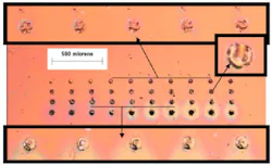
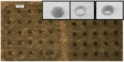
Figure 6A shows the array of laser–processed, surface-modified 50 micron features on a sol-gel ferroelectric thin film deposited on a Si-wafer and annealed at 7000C for 1h. The data shows a continuous change in surface morphology with increasing laser fluence from 0.849 J/cm2 to 4.244 J/cm2. Spots micromachined at or above 3.4 J/cm2 show ablation. Similarly, Figure 6B shows an optical/SEM photograph, top view, of laser micromachined capacitor arrays. Fully micromachined capacitors can be consistently generated by using varying numbers of laser pulses. SEM micrographs are shown in Figure 6B for a series of arrays machined using varying numbers of laser pulses. The depth of microfabricated capacitors varies from 4 microns to 70 microns, depending on the number of laser pulses. Tuning the surface morphology/thickness with proper laser fluence allows us to fabricate new tunable 3D devices.
FIGURE 6A. Optical photograph of 5x10 array of 50 microns spots. Insets: enlarged ph otographs.
FIGURE 6B. Optical photograph and SEM micrographs of laser micromachined capacitor arrays.
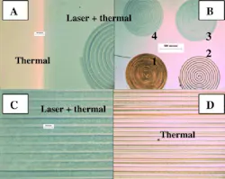
Moreover, an improved laser technique was developed to control the surface morphology and 3D patterning of sol-gel thin films. Surface morphological changes are monitored using optical microscopy. Figure 7 shows different surface morphologies, generated by variation of laser fluence, on laser-annealed sol-gel barium titanate thin film. Sufficiently strong laser pulses induce local melting and rapid cooling, leading to formation of "wavy" 3D structures. One can use laser irradiation to raise the temperature of the film above the crystallization temperature, but below the melting temperature, thus generating a regular 3D pattern.
Figures 6A and 7 represent typical examples of melting and solidification of thin films. Ablation was observed at higher energy densities. With a gradual decrease in energy, but still at high enough fluence values, the central part of the area traced by the laser beam path completely melts, whereas the adjacent surrounding area appears to be a partially melted patterned surface. Figures 7A-B show a variety of spiral patterns generated at a laser-annealed surface. Figure 7B, spot 2, shows a laser ablated spiral pattern obtained at a fluence of 1.69J/cm2 , beam velocity of 100 mm/s, pulse repetition rate of 30 kHz, 4 repetitions, and radial pitch (distance between adjacent traces within the spiral) of 462.5 µm. The laser selectively removed (ablated) film and generated spiral pattern. Decreasing the radial pitch to 4.62 microns at 30 kHz pulse repetition rate results in complete removal of the film (spot 1). At lower fluence (0.679 J/cm2), with a radial pitch of 4.62 microns, the film interacts with the laser, but the pattern was not uniform (spot 3). At this low fluence with higher radial pitch (46.25 microns) a uniform 3D spiral pattern results (spot 4). These patterns are interacting with the visible light and show significantly different localized color than the bulk film. The effect of laser fluence on laser-thermal annealed and thermally annealed surfaces was also investigated. Figures 7C and 7D represent 3D patterns on laser-thermal annealed and thermally annealed surfaces, respectively. Rastering at low laser fluence (0.679 J/cm2) with a 50 micron spot size can generate more uniform pattern at the laser-thermal annealed surface than on the thermally annealed surface.
FIGURE 7. Laser micromachining on laser-thermal and thermally annealed film deposited on Si-substrate.
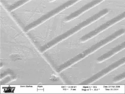
Laser micromachining of printed conductors has also been explored. Nanococomposites are attractive for resistor/laser/capacitor/conductor etc. applications because variable property materials can be formed simply by changing the filler polymer ratio. These compositions, however, have practical advantages only when they are capable of being printed in the internal layers of circuit boards. It can be seen that screen and ink-jet methods can produce line features in the range of 75-100 microns (Figure 2A-2H). Laser micromachining of printed conductor surfaces can produce finer features (Figure 8).
FIGURE 8. SEM micrograph of laser micromachining on conducting surface.
Conclusions
A variety of micromachined surfaces suitable for multifunctional capacitor applications has been demonstrated. Lasers can provide various complex micromachined patterns. This technique can be used to prepare capacitors of various thicknesses from the same capacitance layer, and ultimately can produce variable capacitance density, or a library of capacitors. The process is also capable of making vertical 3D multilayer embedded capacitors from a single capacitance layer. Vertical multilayer capacitors are particularly beneficial for thicker capacitor layers, as could be used in high speed applications where the thickness of the dielectric material in which the capacitors are embedded is, in general, greater. Laser micromachining can produce a variety of random as well as regular 3D patterns. Laser micromachining performs better at laser-thermal annealed surfaces than only thermally annealed surfaces. Laser micromachining is useful for developing finer printable features. As the demand grows for complex multifunctional embedded components for advanced organic packaging, laser micromachining will continue to provide unique opportunities. The strategy presented here may be extended to other nanomaterials suitable for microelectronics packaging.

