KIT develops "photonic wire bond" for optical chip connections
September 27, 2012 - Researchers at the Karlsruhe Institute of Technology (KIT) say they have developed a novel optical connection process for semiconductors using "photonic wire bonding" and femtosecond lasers, that achieves data transmission rates of several Tbit/sec.
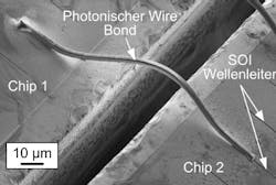
Developing and integrating high-performance optical emitters and receivers onto semiconductors is already a reality, but it's been harder to figure out how to actually bridge chips optically. "The biggest difficulty consists in aligning the chips precisely such that the waveguides meet," explains Christian Koos, professor at the KIT Institutes of Photonics and Quantum Electronics (IPQ) and of Microstructure Technology (IMT) as well as member of the Center for Functional Nanostructures (CFN).
So he and his team looked at the problem from the other side: arrange the chips and then structure a polymer-based optical waveguide. They developed a method for 3D structuring of an optical waveguide using high-resolution, two-photon polymerization -- a femtosecond laser writes the freeform waveguide structure directly into a polymer on the surface of the silicon-on-insulator chips. (Specifically they used laser lithography from Nanoscribe, a KIT spinoff.) Importantly, this means the interconnection adapts to the chip's position and orientation, so such restrictive alignment isn't necessary from the beginning -- making this process more suitable for industrial production scale-up.
Prototypes of the photonic wire bonds were said to have very small losses and very high transmission bandwidth in the range of IR telecommunications (1.55 μm wavelength), and experiments have demonstrated data transmission rates exceeding 5 Tbit/sec. Potential applications are in complex emitter-receiver systems for optical telecommunications, and sensor and measurement technology.
The research is described in the July 30 edition of Optics Express.

About the Author

James Montgomery
Associate Editor
James manages editorial production for news (online and print) and newsletters, as well as the magazines' new product sections. Jim has 13 years’ experience in producing Web sites and e-mail newsletters in various technology markets for CNet, ZDNet, Digital City Boston/AOL, and KM World.