Laser patterning of transparent electrode films: from solar panels through high-end displays

Picosecond lasers deliver better results than typical scribes
By Ralf Hellmann and Colin Moorhouse
The availability of an expanded range of laser pulsewidths and wavelengths enables patterning of transparent conductive oxides to be optimized for applications as disparate as solar cells and OLED displays.
Introduction
Thin films of transparent conductive oxides (TCOs) are used as electrodes in applications where light must pass through the electrode, such as on the front side of certain solar cell types as well as in flat panel displays. Often, these conductive films must be scribed through to create a pattern of electrically isolated areas. Until now, the Q-switched nanosecond laser has dominated these applications, but the advent of newer displays, particularly those based on OLED technology, is creating a demand for even higher quality scribes. The authors have investigated the use of a picosecond laser for this purpose. This article presents the results of this testing which shows that picosecond lasers can deliver results which are superior to typical scribes created by ultraviolet nanosecond lasers.
Scribing: The need for patterned electrodes
Thin films of materials such as indium tin oxide (ITO), gallium zinc oxide (GZO) and aluminum zinc oxide (AZO), demonstrate good conductivity, yet are essentially transparent at visible wavelengths. This makes TCOs very useful for devices which require electrodes placed on a front surface through which light must pass. Typical examples are thin film solar panels and touch screen displays.
TCOs are typically formed as continuous films which must then be subsequently scribed through in order to form the required pattern of electrically isolated electrodes and interconnects. Originally, this was accomplished by photoetching using wet chemicals. However, laser scribing offers several advantages. It is a simpler, single step process that employs no wet chemicals, and which delivers high process flexibility. These advantages of the greener laser process have led to its adoption in most applications.
Nanosecond lasers for solar and touchscreens
Currently, most high volume TCO scribing applications rely on nanosecond, Q-switched, diode-pumped, solid-state (DPSS) lasers such as the Coherent AVIA and Matrix series. These lasers are available with a choice of infrared (1.064 µm), green (532 nm) or ultraviolet (355/266 nm) outputs. Despite TCO’s transparency at visible wavelengths with tight focus and high laser fluence, visible, Q-switched lasers can scribe these films with similar results as infrared lasers with sufficient quality for current, commercially available flat panel displays.
The highest quality scribes are created using ultraviolet lasers – see FIGURE 1. But today, most TCO scribing is actually performed using either infrared or green DPSS lasers as they both deliver the requisite scribe quality without incurring the higher cost of ultraviolet lasers and their more expensive beam delivery optics. The exact influence of laser wavelength on scribe quality depends on which TCO is being used, and for some, the increased quality available from ultraviolet lasers justifies their use.
With regards to process geometry, some applications scribe from the TCO side of the panel whereas others reach the material by passing through the substrate side. The latter enables TCO scribing even after another layer has been deposited on top of it. But with this back-side processing configuration, care has to be taken to avoid damaging the substrate, since this may be exposed to high laser fluences.
Picosecond lasers for OLED screens
Some emerging, high volume applications, most notably OLED displays, are now putting higher demands on scribe quality beyond just electrical isolation, which in turn requires a more detailed examination of scribe geometry and hence quality. FIGURE 2 schematically illustrates the difference between the cross sections of an ideal scribe and a real world laser scribe. The ideal scribe is characterized by complete removal of the TCO layer for electrical isolation, a clean top surface with no shoulders or recast material, a flat bottom with no residual material and no damage sustained by the substrate. In addition, grooves with upright (vertical) sides are preferred as they deliver the highest electrical isolation for the narrowest overall scribe width. In contrast, real scribes created by nanosecond lasers may have shoulders, a round bottom and some recast debris.

Even where these scribes exhibit complete electrical isolation, any high shoulders or ridges are unacceptable for emerging OLED applications, in part because of the dimensions of the top layer that is deposited over the TCO. Specifically, the organic active layer on top of the TCO in an OLED is often only 100 nm in total thickness. So TCO ridges approaching 100 nm in height create the risk of unacceptable shorts through this top layer.
This situation is thus driving the need for an alternative laser scribing method that can produce more nearly perfect scribe characteristics. To this end, the author’s research group at the University of Aschaffenburg has conducted extensive testing using a novel picosecond laser source; the Coherent Talisker ultrafast laser. This is a one-box, hybrid laser that combines a diode-pumped fiber laser oscillator with a diode-pumped free-space amplifier. This compact configuration provides the low cost and operational simplicity of a mode-locked fiber laser, while delivering the higher power/pulse energy and superior beam quality that can be uniquely generated by a free-space regenerative amplifier.
Picosecond lasers can be expected to provide superior results as most of the undesirable groove imperfections are due to thermal effects. Even with ultraviolet lasers, the material being removed becomes hot before it is ejected. This is because the laser pulse primarily excites electrons in the TCO material. This electronic excitation is then converted to lattice vibration, i.e. lattice heating. With nanosecond and longer pulses, there is sufficient time for some of this heat to flow out of the localized laser interaction zone and cause peripheral thermal effects – the heat affected zone (HAZ). But with laser focal spots on the micron scale, the time for this heat flow is on the order of 10 picoseconds or more. So with laser pulsewidths of 10 ps or less, the laser-driven material removal is completed before significant thermal energy out-flow can occur.
Results of picosecond laser study
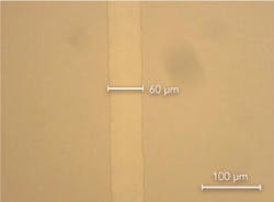
In these studies, we investigated two different TCOs; the more commonly used indium tin oxide (ITO) as well as gallium doped zinc oxide (GZO). To approximate common commercial applications, the TCO was deposited over a thin layer of SiO2 on conventional plate glass substrates (FIGURE 3). The ITO thickness was 150±10 nm, and the GZO thickness was 200±10 nm. In both samples types, the SiO2 barrier layer thickness was 15-20 nm. Scribes were created and evaluated as a function of wavelength using three different Talisker wavelengths; 1064 nm, 532 nm and 355 nm. The effects of pulse energy and scribe geometry were also studied, i.e., scribing from the TCO side vs. the substrate side. We also studied lines of overlapped laser shots (i.e., continuous scribes), as well as single shot ablation. The focused laser spot size was approximately 42 microns in all cases.

1064 nm results
FIGURE 4 shows the excellent scribe quality in ITO when using low (5 µJ) pulse energy and a wavelength of 1064 nm with scribing from the ITO side. (As with other test results shown in this article, these surface profile data are plotted with an expanded vertical scale to exaggerate any roughness and/or debris details.) In particular, there are almost no shoulders at the edge of the scribe, and the surface roughness at the bottom of the scribe is only about 15% higher than the original surface roughness of the unscribed film. The depth of the scribe is slightly greater than the ITO thickness, indicating slight over-etching, which could probably be eliminated by using even lower pulse energies.

FIGURE 5 shows typical results of some single-shot ITO tests at higher pulse energies. At very high (32 µJ) pulse energies, there is much more material ablated when the laser is applied from the substrate side. The extra processing power in this configuration is almost certainly due to an effect called spallation which happens with pulsed lasers and high fluences when intense absorption occurs at an enclosed interface, and there is nowhere for the expanding vaporized material to escape. The resultant sudden expansion of atomized material creates a shock wave that blows off the thinner of the two layers.

Better single shot results were obtained by using lower pulse energy and ablating from the substrate side; witness the excellent example in FIGURE 5c obtained with a pulse energy of 10 µJ.
In the case of GZO and 1064 nm processing, front side scribes showed larger shoulders (up to 50 nm) and rough groove-bottom surface. This occurred even when the pulse energy is only 10 µJ (i.e., 1.44 J/cm2). This can be attributed to the higher heat conductivity of ZnO as compared to ITO.
532 nm results
As with the 1064 nm wavelength, we found that when using the Talisker laser’s 532 nm output, the best scribing results (lower roughness and smaller shoulders) were obtained when ablating from the substrate side and using low pulse energies (10 µJ or less). (At pulse energies above 10 µJ, we observed substrate damage.) FIGURE 6 shows typical surface profile data for scribes produced by front-side irradiation of ITO with 10 µJ pulse energy. Notice that the shoulders are almost non-existent, the groove walls are quite vertical and the roughness at the bottom of the groove is only slightly higher than for the unprocessed surface. The only negative is that the groove is about 25 nm too deep, but this can be avoided by lowering the pulse energy.

GZO did not ablate well at with the 532 nm laser output. For example, with front-side irradiation at 532 nm, even pulse energies as high as 20 µJ produced no ablation of the GZO. However, this configuration did result in substrate damage, even though the laser was incident on the front-side.
355 nm results
With ultraviolet laser wavelengths, the scribing of ITO is more efficient in terms of material removal than at other wavelengths; however, it produces inferior quality results. In part, this is because the scribing has to be from the front side because of the UV absorption characteristics of the glass substrate. For example, FIGURE 7 shows a cross-section profile through a continuous scribe in ITO obtained with just two passes and pulse energy of only 4 µJ (i.e., 0.58 J/cm2). The groove has good depth and vertical sides but the shoulders can be as high as 30 nm.

In contrast, the GZO machined much more efficiently and with better quality results in the UV than at longer wavelengths. We found that it is important to minimize the pulse energy to avoid cracks in the bottom surface of the scribe; small cracks occurred even at 5 µJ (i.e., 0.72 J/cm2), and at 10 µJ (i.e., 1.44 Jcm2) these were clearly unacceptable.
Results summary
To summarize, in terms of the “ideal scribe” target result, many of these picosecond test results were markedly superior to the typical nanosecond results shown in FIGURE 2. Better results were universally obtained when scribing from the substrate side rather than the TCO side. And ITO generally machined much more easily and produced better scribes than did GZO. The ITO machined best with IR and green wavelengths. But we also found that pulse energies must be kept low to avoid substrate damage. The GZO requires UV laser processing which also necessitates front-side scribing. Here pulse energies had to be kept low to avoid cracking of the substrate at the bottom of the scribes.
Fortunately, ultrafast lasers such as the Coherent Talisker are characterized by very high pulse repetition rates (up to 200 kHz). So, although our results show that TCO scribing clearly is optimized with low pulse energies, the high repetition rate means that even with 5 µJ pulse energies, high pulse-to-pulse overlap and multiple passes, scribe speeds as high as 250 mm/s are sustainable in production settings. At higher pulse energies (e.g. 10 µJ pulse energy 1.44 J/cm2 fluence) isolating lines can be scribed at up to 2000 mm/s. (Of course, this general picture varies at the three wavelengths and also the results exhibit different quality levels.)
Conclusion
Nanosecond DPSS lasers currently still dominate scribing of TCOs in volume applications. In a single dry step they create scribes that deliver complete electrical isolation and require, at most, only minimal post-processing. But new applications in high-end displays are demanding higher quality scribes. As demonstrated here, picosecond lasers are able to deliver the requisite quality and because these lasers are now available at amplified power levels, they can deliver cost-competitive scribe speeds. In fact, in addition to new OLED applications, the authors know of several existing solar applications who are now evaluating whether to switch to these new lasers.
Ralf Hellmann ([email protected]) is a professor at the Aschaffenburg University of Applied Sciences (Germany), and Colin Moorhouse ([email protected]) is with Coherent Inc. www.coherent.com.