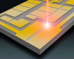
Laser ablated solder trenches
Westford, Mass. – Laser Services, a high powered laser job shop and materials distributor, has released an ongoing series of Technical Briefs that introduce laser techniques to engineers not familiar with the advantages of laser cutting, drilling, and scribing over traditional machining methods.

The first installment, "Keeping Solder in Its Place with Laser Ablation," describes a laser-based method that produces a clean, precision trench around solder pads. When the proper setup is achieved, exacting amounts of power remove only the layers of top material (typically Au/Ni) needed, exposing the mid-layers that form the trench without exposing sensitive base materials. Laser Services can also control the laser to ablate through and over edges of the PCB, again without impacting important base materials.
The laser machining systems at Laser Services are compatible with standard computer-aided-manufacturing (CAM) and computer-aided-design (CAD) circuit artwork files. The fast processing speeds of these computer-controlled systems translate to fast PCB turnaround times and low production costs.
Laser ablation is also useful for a variety of other tasks, including repairing PCBs by removing conductive traces without damaging surrounding areas. It can also be used for machining dielectric and copper materials to form unique surface features such as chamfers around cutouts. The fine resolution of lasers also delivers high isolation even on densely populated PCBs.
For small-piece orders or large production runs, laser ablation provides the flexibility and processing speeds for a wide range of PCB manufacturing applications. Laser ablation is incredibly accurate and forms solder dams with less material and less labor than any other PCB solder damming process.
Laser Services is an ISO and AS-9100 registered laser cutting, drilling, scribing, etching, and welding services provider. The company specializes in processing ceramic substrate (alumina) materials and a variety of other PCB substrates. A fully equipped 16,000-sq.-ft. facility features 25 low-to-high-power lasers and a wide range of state-of-the art processing tools.
For more information, contact Tara Graham, [email protected].