Pulsed laser deposition system enables chip, material creation with larger patterning areas

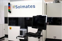
The University of Twente's MESA+ nanotechnology research institute (Enschede, The Netherlands) has purchased an advanced pulsed laser deposition (PLD) system from spinoff company Solmates, a research partner of the institute.
The new device will allow the institute to create new materials and chips (or individual chip components), which are constructed as a series of one-atom-thick layers. Since the MESA+ NanoLab's researchers and external users will now be able to work on an industrial scale, new scientific knowledge in the areas of unconventional electronics and advanced materials will be more accessible, as well as more suitable for practical application at an earlier stage.
The MESA+ NanoLab's work centers on creating extremely thin layers consisting of just a single layer of atoms. This involves using a laser to transform a material into a plasma, which then condenses on a surface to form an extremely thin layer. By layering multiple very thin layers, one over the other, it is possible to create completely new chips (or individual chip components) and materials with properties never seen before. Arjen Janssens, CEO of Solmates, expects that by around 2020, the PLD technique (which was partly developed at the University of Twente) will have evolved into one of the standard chip production systems.
The limitations of the equipment previously used for this purpose at universities meant that it was only possible to process relatively small areas (10 × 10mm), but the new system at the MESA+ NanoLab allows laying down patterns across much larger areas. Now, they can lay down patterns on 20-cm-diameter wafers, which means that the institute's research results—and the novel technology it creates—will be directly applicable in industry. Moreover, the new equipment is much more user-friendly, so many more NanoLab users will be able to use it.
For more information, please visit www.utwente.nl/mesaplus.