Laser processing of thin films
A laser is used to produce the isolating tracks immediately prior to capacitor winding
Mike Osborne and Andrew Webb
The stereotypical lifestyle of the developed world now revolves around cheap electronic devices, many of which cram amazing functionality into very small physical form-factors. Examples include mobile phones, portable music players, GPS devices, PDAs, and laptop computers to name a few (see Figure 1).
Central to this has been the ability to shrink the individual electronic components that compose these devices. The component that has received the majority of the attention in this miniaturization has been the transistor in its various forms. The principles of operation of this active device rely on the electrical properties of doped materials almost at the atomic scale. This has allowed active dimensions to be measured in tens of nanometers, with integrated circuits now routinely available containing transistors with 45nm gate dimensions, allowing hundreds of millions of transistors to be produced on a single chip.
While the shrinkage of active devices has been a huge technical success, and led to enormous commercial opportunities, there are a range of other electronic components where the miniaturization process is more problematic due to the physics of device operation. Capacitors and inductors are good examples. In these devices, the capability of the device is inherently governed by physical (macroscopic) parameters. This is obvious from the simple equations describing capacitance and inductance. The equations show how the values depend explicitly on the geometric properties of area (A), distance (d), and length (l) for a parallel plate capacitor and a solenoid inductor.
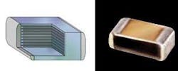
The geometric determinant of the capacitance is explicitly visible in the construction of thin-film capacitors, as illustrated for a surface mount device shown in Figure 2.
Although other forms of capacitors exist that have potentially higher energy densities, the simple multiple-layer parallel plate capacitor still has advantages in terms of frequency response and equivalent series resistance (ESR), which make it the design of choice in many applications.
In order to minimize the size of the electronic device, it is necessary to minimize the macroscopic discrete components such as the capacitors and inductors. The most successful approach currently employed is surface-mount technology, which not only eliminates the need for wire connectors, but is also more suited to automatic population of circuit boards.
The physical format of miniature surface mount capacitors is traditionally referred to by a code which gives the x-y dimensions of the capacitor in hundredths of an inch. Hence a 0402 series capacitor measures 4 hundredths by 2 hundredths (or 1 x 0.5mm).
In practice, the structure of a thin-film capacitor is formed from many layers of polymer film, which is coated with a metal. Typically the metal is aluminum, and there are various possible choices for the polymer including polypropylene (PP), polyester (PE), polystyrene (PS), and polyphenylene sulfide (PPS). A schematic of this is shown in Figure 3 (for illustration purposes, this shows an artificial separation between the individual layers).
In traditional manufacturing techniques, this structure is produced by co-winding two reels of metalized polymer film that already have the isolating track. As the value of the capacitance is directly related to the distance between the isolating tracks, the electrical properties of the capacitor are dependent on how accurately this spacing can be maintained over the many hundreds of layers that make up the capacitor. As the dimensions of the capacitor are reduced (and the electrical tolerances tightened), maintaining the accuracy of the winding becomes a severe technical challenge. This is compounded by the inherent difficulty in handling such thin materials which, if stretched, will break the electrical continuity of the metalized layer, thereby ruining the electrical performance of the capacitor.
A further limitation of the traditional manufacturing approach relates to how the isolation tracks are produced in the first place. Conventionally this is done using a contact mask during the metalization of the polymer film. This mask is inevitably in the form of a fine “string” that is laid on the material. Once the metalized layer is deposited, the “string” is mechanically removed, leaving the isolating track.
In production there are limitations on how small the “string” and hence how thin the insulating track can be. This leads to larger than necessary tracks, and the resultant wasted real estate within the capacitor. The resulting mask is extremely thin and flexible, making it difficult to handle and easy to stretch, damage, or break. Also the removal of the mask tends to tear and delaminate the metalization
OpTek Systems has developed an alternative manufacturing technique in which a laser is used to produce the isolating tracks immediately prior to the winding of the capacitor. This has a number of significant advantages, including: optimized track width, leading to further miniaturization and less wasted real estate; easier winding; better capacitance accuracy; reduced layer-to-layer variations; and reduced consumables costs, as pre-isolated tape is not needed and JIT manufacture reduces the need for stocking multiple demetalized tapes.
OpTek provides systems and services for precision laser materials processing (micromachining), specializing in the area of transitioning challenging laser applications into high-volume production. The company is not a manufacturer of lasers so it is not biased in the direction of any specific laser type, but employs what is considered to be the most appropriate laser and set of processing parameters for any given application.
There were several technical challenges to achieving the desired performance goal. These can be grouped under the following three headings.
Substrate damage
In the capacitor, the polymer acts as both the insulator and dielectric. Thus, to maximize the capacitance for a given volume of capacitor, the polymer is generally kept as thin as is electrically possible, highly stressing the dielectric. Clearly, the insulation (voltage hold-off) properties of the polymer cannot be compromised by the laser process. Moreover, the dielectric response at all potential operating frequencies cannot be altered. Given the thinness and hence fragility of the material, these requirements place a significant challenge on the laser process.
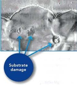
These issues were compounded by the fact that the base polymer film was found to contain very small silica particles (spheres), which are deliberately introduced during the manufacture to improve the mechanical “slip properties” of the film, making it easier to handle and wind. In optical terms, these particles act as ball lenses over a wide range of wavelengths, potentially producing large local variations to the applied laser intensity. Alternatively, they can be removed explosively, leaving damage to the substrate (see Figure 4).
Field enhancement
Any sharp edges to the metalization will reduce local electric field enhancement, reducing the effective voltage rating of the capacitor. The edge of the metalization is unavoidable, but any serrations, filaments, or metalic debris particles will give field enhancement, and so need to be avoided (see Figure 5).
null
Winding considerations
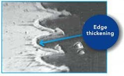
Finally, the laser process must not affect the ability to wind the hundreds of layers which make the capacitor. In this respect, thickening of the metalization at the edges is not allowed (see Figure 6).
With the appropriate choice of laser processing parameters, all of the above negative effects can be avoided.
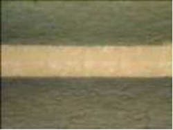
Figure 7 shows a 20µm wide demetalized track on a 1.2µm thick substrate. As can be seen, there is no damage to the substrate; the track’s edges are free from serrations and edge-thickening; and there is no apparent debris.
This capability has been integrated into a production winding machines and is used in production at ~10M capacitors/year per machine. The photovoltaic industry is adopting this technique of laser demetalization for high-volume manufacturing of printed flexible solar cells.
Mike Osborne ([email protected]) is with OpTek Systems, Abingdon, UK, and Andrew Webb is with OpTek Systems Inc. (www.opteksystems.com), Greenville, SC.


