Laser chemical processing
A PROVEN SOLUTION FOR THE MANUFACTURE OF SELECTIVE EMITTER SOLAR CELLS
R. SCHMITZ AND A. PAUCHARD
One of the current developments in the field of silicon solar cell technology is the implementation of selective emitter structures. Research to find a suitable technology for the mass production of cells with selective emitters has been an ongoing activity for many years and, over the last two years, industrial solutions have been commercialized by a number of suppliers. The main function of the selective emitter is to minimize and localize the highly doped area to the minimum – this is below the contacts. Few of the selective emitter technologies reduce in parallel the contact area. And only one of these technologies, the LCP based RENA selective emitter, is completely self adjusting using the whole potential of the technology. This way the blue response, open-circuit voltage and the fill factor of the cells with the selective emitter structure can be improved, leading to an efficiency improvement of 1% and more.
One of the most promising technologies for the industrial production of selective emitters is laser chemical processing (LCP). It is a laser technique that satisfies several applications in solar cell fabrication including microstructuring, wafering and doping1. It was proposed by Willeke and Kray in 20012 and is based on the liquid jet guided laser system LaserMicroJet®, invented by Richerzhagen3, patented and commercialized by the company Synova SA of Switzerland. The principle is to couple a laser beam into a laminar liquid jet in which it is guided onto the work piece by total internal reflection at the jet surface. LCP extends the system by using different chemicals instead of water as a liquid jet. Here the laser beam can thermally treat the material or it can trigger photochemical or thermochemical reactions.
LCP is able to perform local diffusions at high speed and accuracy without the need of masking or any high-temperature step of the entire wafer. Doping is possible with a liquid jet containing the dopant compound. Here the silicon is melted by laser irradiation and the molecules in the liquid dissociate and diffuse into the silicon melt. Developed at the Fraunhofer Institute ISE in Freiburg, Germany, the technology is now being sold exclusively through Rena GmbH of Germany. Synova and Rena have recently formed a joint venture for the commercialization and further development of the LCP technology, named RenaSynova Wet Laser GmbH.
Combining selective emitters and light-inducing plating
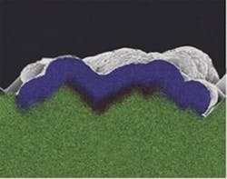
A significant improvement of the solar cell properties can be achieved when combining selective emitters (SE) produced by LCP and metallization produced by light-induced plating (LIP), as shown in FIGURE 1. The combination of SE and LIP provides an efficiency increase of +0.9% absolute4. Meanwhile, the RENASynova group has achieved 1.2% in the lab and RENA offers 1.0% for standard applications. This increase in efficiency represents a significant step towards achieving grid parity.
The selective emitter solution uses two effects to increase the cell efficiency. The first is the geometrical effect by using contact fingers with 50 μm contact width instead of 120 μm for printed contacts. The additional active area increases the efficiency by around 0.5%. The other part of the efficiency increase is due to the enhanced blue light response, an effect caused by the lower doping level in the active area.
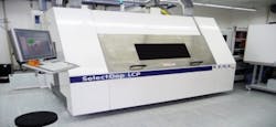
A liquid-guided laser beam opens 35 μm width lines in the SiN passivation layer. By using diluted phosphorous acid as liquid, a simultaneous, self-adjusted n++ doping takes place in the openings. The following NiAg plating into the openings is also a self-adjusted process so that no misalignment is ever possible. Machines with a throughput of more than 2400 wafers/hour are already available from Rena GmbH, as shown in FIGURE 2.
The LCP technology can also be implemented for p-type doping as local back surface field in low cost high efficiency silicon solar cells. Local p-type doping is usually used as local back surface fields for p-type solar cells, such as laser-fired contacts5. The LCP technique provides the opportunity to create local doping both at the front side and the rear side of a solar cell. These kinds of doping can be created with the use of a liquid boron source. Kluska et al. recently demonstrated successful local p-type boron doping using the LCP process. The doping medium was an alkaline aqueous boron solution. A peak doping density of 1020 cm-3 and a doping depth of about 1 μm were obtained. Furthermore, the intentional variation of the pulse energy leads to sheet resistances in the range of 25 Ω/sq to 230 Ω/sq6.
A detailed understanding of the LCP process was obtained by the Fraunhofer ISE research team using advanced simulation techniques7, taking into account the real laser light intensity profile within the liquid jet cross section. The comparison of the simulated doping profile and a SIMS measurement on a sample processed by LCP shows good agreement. The numerical model is able to describe the LCP doping process in realistic way and can be used to analyze the dopant distribution in more detail. The simulation tool can further be used to predict the impact of various process parameters, enabling a fast development iteration time.
Conclusion
The LCP technology has evolved quickly to become one of the most promising solutions for the selective doping of solar cells. In-line machines with low total cost of ownership are already available for front-side doping and metallization. Simultaneous SiN ablation and phosphorous doping by a liquid jet guided laser, combined with self-adjusted NiAg plating, already provide an efficiency increase of 1% absolute. The process is fast, fully automated and does not require the use of any masks and alignment.
Further advanced solutions for backside p-type doping are being investigated at Fraunhofer ISE and promising results have already been demonstrated. The LCP technology could soon be the technique of choice for the introduction of dopant into the front and backsides of solar cells.
References
1. D. Kray, A. Fell, S. Hopman, K. Mayer, G.P. Willeke and S.W. Glunz, "Laser Chemical Processing (LCP): A versatile tool for microstructuring applications," Applied Physics A, Volume 93, pp. 99-103, 2008.
2. G.P. Willeke, D. Kray, "Proceedings of the 17th European Photovoltaic Solar Energy Conference," Munich, Germany, p. 1621, 2001.
3. B. Richerzhagen, Entwicklung und Konstruktion eines Systems zur Übertragung von Laserenergie für die Laserzahnbehandlung, 1994.
4. D. Kray et al., "High-efficiency large area industrial LCP selective emitter solar cells ready for production," Proceedings of the 25th European Photovoltaic Solar Energy Conference and Exhibition, 5th World Conference on Photovoltaic Energy Conversion, pp. 1896-1898, 6-10 September 2010, Valencia, Spain.
5. E. Schneiderlöchner, et al., "Laser-fired rear contacts for crystalline silicon solar cells," Progress in Photovoltaics: Research and Applications, 10: p. 29-34, 2002.
6. Kluska et al., "Analysis of local borong dopings formed with LCP," Proceedings of the 25th European Photovoltaic Solar Energy Conference and Exhibition, 5th World Conference on Photovoltaic Energy Conversion, pp. 1405-1409, 6-10 September 2010, Valencia, Spain.
7. Fell et al., "Investigation on the influence of the intensity profile on the doping quality in laser chemical processing," Proceedings of the 25th European Photovoltaic Solar Energy Conference and Exhibition, 5th World Conference on Photovoltaic Energy Conversion, pp. 1796-1799, 6-10 September 2010, Valencia, Spain.
R. SCHMITZ([email protected]) and A. PAUCHARD([email protected]) are both with Synova, Ecublens, Switzerland.
More ILS Current Issue Articles
More ILS Archives Issue Articles


