Reel-to-reel machining using ultra short pulsed lasers

HIGH MATERIAL THROUGHPUT WITH LOWEST MANUFACTURING COSTS FOR STRUCTURING OF THIN FILMS
CHRISTIAN SCHOLZ
The continuing growing demand for high yields and mass production of flexible electronic devices requires new production processes based on industrial systems combining high throughput with extremely low manufacturing costs.
An example is a reel-to-reel laser system, developed by 3D-Micromac AG, which meets the demands of these goals. With this system, on-the-fly processing of continuously moving flexible substrates is enabled through the integration of a laser source into a reel-to-reel tool.
The investigation of laser processing of thin films on top of flexible substrates was performed for applications in the field of electronic devices and flexible solar cells. For these purposes, ultra short pulsed lasers prove to be ideal for the ablation of heat sensitive thin films because of their short interaction time with solid state bodies (nearly non-thermal ablation by minimization of energy introduced to the photonic system). Furthermore, an interaction with the ablated plasma is nearly absent because of lack of coincidence. All these facts result in a minimum of stress at the borders of laser processing and generation of a minimal heat affected zone.
Structuring of flexible circuitry
To make flexible electronics available for the mass market, they have to be fabricated in low-priced processes. Printed circuits are cheaper than those achieved through chemical or physical deposition processes. Unfortunately, there are technological process steps which cannot, or only with great effort, be covered by available printing technologies. For example, the generation of high quality interconnects for the production of double-sided polymer circuit cards or thin film systems can hardly be achieved using established processes such as punching. With the integration of a direct writing laser process, steps not covered by conventional methods can be realized without restrictions to the continuous reel-to-reel web handling.
A typical example for a printable conductive layer material is the conductive polymer PEDOT:PSS. In the wavelength range between 330 nm and 1100 nm, this material has a very low degree of absorption, which is only insignificantly higher than the commonly used PET substrate. This property impedes a laser-based ablation of this layer without influencing the substrate. Therefore, machining tests on the ablation behavior of PEDOT:PSS on top of a PET substrate with different laser wavelengths (266-1064 nm) and pulse durations (12 ps-100 ns) have been carried out. First, different lasers with 1064 nm wavelength and different pulse durations between 12 ps and 100 ns were used. As expected, initial tests with wavelengths in the range of the visible light and IR indicated that the PEDOT:PSS layer cannot be machined before inducing significant damage to the substrate. Based on these experiences, tests with a wavelength in the range of UV (355 nm) were carried out on paper and foil as carrier substrates. Though the layer could be completely removed by applying a laser source with a pulse duration of 50 ns, the PET foil was damaged (blistering).
The application of ultra short pulsed laser beams enables the ablation of the functional polymer without the blistering effects of the foil. Using a laser fluence that allows an appropriate isolation of the thin film polymer layer, a small amount of less than 10 μm of the substrate material was removed. This material ablation is not critical in various applications, e.g., when isolation between two conductive areas has to be achieved. The cutting speed depends strongly on the cutting geometry. The laser-related limitation was reached at a cutting speed of 5 m/s using a repetition rate of 640 kHz and generating a cutting width of 28 μm. An additional increase in the cutting speed can be achieved by applying laser sources with higher repetition rates.
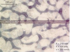
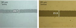
The depth of the trenches in the substrate material could be reduced further by use of a wavelength of 266 nm and pulse duration of up to ~ 2 μm (FIGURE 1). This result is based on the fact that the absorption of the PEDOT:PSS and PET substrate below 330 nm wavelength increases significantly, reducing penetration depths. The disadvantage is that the output power of the laser source is also further decreased, and the requirements for producing the optical path are increased tremendously.
The machining of PEDOT:PSS layers on paper substrate are less critical because of the better thermal stability of the substrate material. Therefore, the process window for the ablation of the polymer layer is increased as the substrate is not damaged before exceeding an energy threshold that is significantly higher than necessary for the ablation of PEDOT:PSS. But, similar to the foil, it can be observed that with smaller pulse duration and wavelength, isolating cuts with less substrate ablation can be achieved.
Structuring of flexible CIS-solar cells
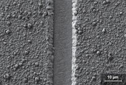
Based on the productivity of reel-to-reel processes, it is also possible to use this method to produce flexible solar cells. Laser machining of CIS-solar cells with ultra short pulsed lasers has been established as a less damaging process for selective ablation of the layers (FIGURE 2). This has already been proven by 3D-Micromac in recent projects.
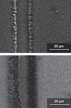
Additionally, an industrial process technology of picosecond laser micromachining up to 1.5 μm thick CIS-absorber layers on polyimide base has been developed. A transaction of the CIS layers can be noticed at energies of about more than 1 μJ. The result is shown in FIGURE 3. The edges of the rills show variances in the microstructure, which indicates that the absorber layer in this 5 μm wide area was marginally melted and solidified afterward.
Based on detailed research using transmission electron microscopy of cross-section compounds (incluing energy dispersive X-ray) and Raman micro-spectroscopy, the ablation selectivity was proven. Moreover, the damage free machining, especially in the case of creating a function-damaging CuxSe phase, was documented.
Laser scribing organic solar cells
A great advantage of conductive and semiconductive polymers is the possibility to deposit them in high throughput coating processes. This feature provides huge potential for future production of low cost photovoltaics. The pattern of the solar cells can either be generated by a structured printing step or, as already established in silicon-based photovoltaics, by high precision laser scribes.
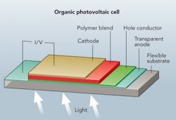
For those scribes, four different laser sources, varying in wavelength, pulse duration and average output power, have been used in the experiment. Two lasers with nanosecond pulses were used, one at 1064 nm with a maximum average power of 200 W, the other at 355 nm with an average power of 20 W. In the ultra short pulse range, a pico- and a femtosecond laser were used. The picosecond laser emitted 1064 nm, 532 nm, and 355 nm with a maximum average power of 40 W (at 1064 nm). The femtosecond laser emitted 1024 nm and 512 nm with a maximum average power of ~10 W (at 1024 nm). All experiments were conducted using high-performance galvanometer scanners in combination with appropriate f-theta lenses. The processed solar cells had a conventional stack layout, which is shown in FIGURE 4.
The patterning of ITO layers is important not only for organic photovoltaics and organic LEDs, but also for more conventional applications such as TFT displays. Lithography is an established process for this task. To overcome the limitations of lithography (new mask for new layout, involvement of various chemicals), some laser patterning tests were done. The first trials involved ITO on 25 mm x 25 mm glass substrates.
A number of problems occur when using nanosecond lasers. First and foremost, the glass substrate is more or less cracked, which is not acceptable in any case. The second problem was the irregular abrasion of the ITO, in part due to both lasers working at their lower power limit. For a stable manufacturing process, constant scribing widths are necessary. As the results were not satisfying, no sample solar cells were built using these structured substrates.
The second trials involved ITO on PET foil substrate with a thickness of ~100 μm. This flexible substrate was handled in pieces that were fixed on a vacuum chuck. Both lasers damaged the PET foil. Though the nanosecond laser at 355 nm worked at <0.5 W, the damage of the PET foil is not acceptable. In addition, the bulge created on the cutting edge is also not compatible with typical post process steps.
Both trials were repeated using the two aforementioned ultra short pulse lasers. FIGURE 5 shows examples of ITO on PET foil.
Though all available wavelengths of the two ultra short pulse lasers were tested, it became clear that 1064 nm is well suited. The scribing quality is as good as with any other wavelength and is also more cost effective. SHG and THG units usually come with an additional price tag and limited lifetime. With these structured substrates, working solar cells could be built that reached a power conversion efficiency of ~2%.
Again, 1064 nm proved to be the best choice, though the other wavelengths also produced acceptable results. Compared to the trials with nanosecond lasers, the pico- and femtosecond lasers only slightly damaged the substrate.
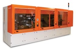
Reel-to-reel standard tool
A standard machining tool for the reel-to-reel process is depicted in FIGURE 6. In this machine rolls up to 600 mm width can be handled.
The on-the-fly work flow requires a combination of image processing of the moving substrate and the laser processing itself. Therefore, image grabbing is accomplished by a modified camera. By using this camera, an automatic recognition of industrial used adjustment marks results. According to the knowledge of the web position, a targeted laser processing is possible.
The illumination for image processing is done by two separate light sources. Diffusers and other optical elements assure an optimal illumination level for opaque and transparent materials. The laser adjustment on the moving web is achieved by a permanent correction of the vector output of the laser scanner. The absence of an on-the-fly correction would generate distortions in the laser processed geometry. Thus, the vector output is controlled according to the web velocity.
The interaction of all these components enables a targeted on-the-fly laser processing of thin films on top of flexible carriers.
Conclusion
This reel-to-reel system offers the possibility to wind and machine various substrates. With the on-the-fly technology, laser machining during the continuous winding process is substrate friendly regarding stretching, and additionally, significantly increases the throughput. As proven in further technology analyses, the high quality requirements in laser machining of flexible circuit carriers and solar cells by using the portrayed reel-to-reel standard machine in combination with ultra short pulsed lasers, can be achieved with very good results.
Acknowledgments
The work presented in this paper has received financial support from the BMBF (German Federal Ministry of Education and Research) within the projects no. 03WKW04A and 13N10315. We would like to thank all our partners in the aforementioned project.
CHRISTIAN SCHOLZ([email protected]) is an R&D engineer with 3D-Micromac AG, Chemnitz, Germany.
More ILS Current Issue Articles
More ILS Archives Issue Articles