Laser processes in PV manufacturing: An update
Corey Dunsky
Potential remains high if at least one laser-based technique is adopted
The possibility that photovoltaic (PV) power conversion could cleanly, sustainably, and affordably power our homes and workplaces has captivated many for over half a century. Today, that vision is rapidly moving toward a reality. With the advent of strong government incentives, primarily in Europe and Asia, the modern PV industry began to take shape in the mid 2000s. At that time, by making PV economics attractive, subsidies stimulated demand and new PV companies emerged that have since scaled production to levels well beyond the projections of a decade ago. The growth rates are nothing short of astounding: annual installations have exploded from 1.46 GW in 2005 to over 17.5 GW last year – a five-year compound annual growth rate of over 65% and up 141% in 2010 over the previous year. On the supply side, 2010 global PV production of panels tallied 20.0 GW, up more than 100% from 2009.

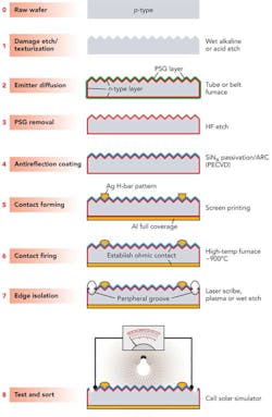
FIGURE 1. Manufacturing process flow for conventional crystalline silicon solar cells.
Though impressive, this growth will be sustained only through a continued steady drive toward price parity with conventional sources of electricity. In 2010, PV module prices (at about $1.75 per W) stood at approximately half of their 2007 value. Much of this price drop can be attributed to both easing of a global silicon feedstock shortage in the late 2000s and massive scale-up of manufacturing infrastructure in low-cost regions. However, innovations in cell design and manufacturing processes have also played a role. Laser processes have drawn intense interest in the past five years as PV manufacturers have pursued some of these new cell architectures. Here, we review how several of those processes have fared over the past 3 to 5 years and offer some perspectives for near-term developments.
PV technology: Two types
Two types of PV technology were brought to market in the past several decades. The first, based on crystalline silicon (c-Si) wafers, commanded over 80% of the market, even as the other, thin-film PV (TFPV) began to fulfill its promise of mass production at significantly lower cost. Due to the nature of TFPV panels, a scribing process is required to divide full-sized panels into multiple series-connected cells. Lasers were the tool of choice from the beginning, and over the past decade laser processing has been adopted as the standard technique for this key step. Today, there is a healthy market for TFPV laser scribing tools, and a number of equipment makers are enjoying considerable success.
Other TFPV laser applications such as edge deletion and glass drilling for panel contact holes are in the evaluation phase. And, as new thin film material systems are developed and mature, there are still opportunities for innovative lasers and laser systems to add enhanced value to the laser scribing process.1, 2
On the c-Si side, the success story for laser processes is yet to unfold. The standard cell and module architectures do not require any process for which lasers are the clear tool of choice. Nevertheless, according to Solarbuzz, in 2010 about 4% of all PV capital equipment sales were of laser-based tools, and industry analysts estimate that about 40% of those sales were for c-Si.3 Because c-Si technology is expected to continue its market dominance for the foreseeable future, the remainder of this article is devoted to a deeper look at emerging laser applications in that realm.
Within the c-Si segment of the PV industry, intensive research and development activities aimed at increasing cell efficiency are being carried out at both commercial manufacturers and public research institutes. The goal is to improve cell performance without significantly increasing manufacturing costs. Toward that end, the baseline process flow shown in FIGURE 1 can be modified by adding new process steps or finding better materials and methods to perform the standard ones shown. How can lasers help to achieve this? We now consider several laser processes that have been developed in recent years to carry out or supplement the process steps shown in FIGURE 1.
Junction isolation: Laser edge isolation
Beginning about 10 years ago, industry researchers explored the laser's potential to quickly and cleanly perform the junction isolation step (FIGURE 1, Step #7). In a straightforward process, the laser digs a groove on the top surface of the wafer, around the cell's periphery. Pulsed lasers emitting in the infrared have been most commonly used, creating a trench about 10 to 30 microns deep and 40 to 80 microns wide. Since any cell area outboard of the groove location cannot harvest sunlight, the groove is placed as close to the wafer edge as possible. The laser scanning speed must be high enough to meet the machine residence-time requirements of conventional PV equipment: no more than about 1.0 to 1.2 sec.
Laser edge isolation (LEI) initially held promise to improve upon the plasma etching process previously used to remove the n-doped emitter layer where it coats the thin edges of each wafer. The LEI concept was quickly proven and commercial tools began to appear about 6 to 7 years ago, now offered by a number of leading laser integrators and established PV equipment makers. Uptake by PV manufacturers was rapid. The process was quickly verified in R&D and pilot production, and ramps to full-scale production have been successfully carried out at major solar companies.
Despite this initial success, the future of LEI is cloudy. Within the past two years, another junction isolation process has gained traction: single-sided wet etching. Though it relies on hazardous chemicals that can be costly to handle, wet etching appears to be overtaking LEI in leading PV companies. The wet chemistry is already present in the plant to perform the damage removal and surface texturing steps, so chemical handling protocols are already in place. Conventional etch tools have been adapted to perform single-sided etching processes more cost-effectively than the LEI tools. Given this technology landscape, the outlook is for some legacy LEI systems to remain in the field in volume PV production, while a limited new-equipment market may persist for 2nd-tier and 3rd-tier c-Si players that are not growing capacity to the gigawatt level. But the tier 1 manufacturers appear to be turning to the wet etch process. Even though the laser process works better than plasma etching, LEI can't compete economically with the newer wet-etch technology.
Laser drilling for wrap-through cells
In a significant departure from the standard cell architecture, wrap-through cells relocate some or all of the metal contacts from the top side of the wafer to the rear. A concept that has been in R&D for about two decades, this approach frees up more sun-side surface area to generate charge carriers, resulting in modest efficiency gains.
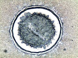
FIGURE 2. Laser fired contact created by a single laser pulse. Aluminum-silicon alloy is obtained in the central region. (Courtesy Fraunhofer ISE)
Two variants have been explored. In the metal wrap-through (MWT) architecture, the heavy busbars are moved to the back, leaving the thin metal fingers on the top side. In the emitter wrap-through (EWT) version, both busbars and fingers move to the rear of the wafer, leaving the sun-facing top surface completely free of metallization. Both techniques rely on holes drilled through the wafer to conduct charge carriers to the rear side, and laser drilling is an effective way to produce those holes. The drilling is performed at the front end of the cell manufacturing flow (prior to FIGURE 1, Step #1), permitting localized laser-generated damage to be removed with the standard saw-damage-removal etch. Since wrap-though cells have all their contacts on the rear side, cell-to-cell electrical connections differ from those of standard modules and the cells must therefore be paired with new module designs. Conventional module-making equipment cannot be used, and the lack of specialized equipment has been one barrier slowing commercialization of wrap-through architectures.
MWT. Of the two wrap-through concepts, MWT is the easier to realize and one manufacturer, Solland, is in small-scale commercial production while a handful of other PV companies are evaluating prototype designs. Laser drilling requirements are modest: in Solland's MWT cells, sixteen 200-micron holes are drilled with a trepanning technique, followed by ablation of an isolating trench surrounding each hole. Utilizing a 60 W commercial TEM00 IR laser, the entire process is completed in 0.9 sec. Cell performance gains are also modest, with an absolute efficiency increase, Δη, of about 0.3%.4 Because this level of efficiency enhancement is comparable to that which can be achieved through improved materials or architectures which depart less from the standard cell, MWT panels are not expected to capture significant market share in the foreseeable future.
EWT. Emitter wrap-through cells hold promise to achieve Δη > 1% and permit use of cheaper, lower-grade silicon, but are more complicated than MWT cells. EWT requires roughly 0.5 to 1.0 wafer penetrations per mm2. For a standard-sized wafer, this means about 25,000 via holes must be drilled, with a total process time of less than 1.5 sec. Percussion-drilled vias 40 to 70 µm in diameter have been created with a high-power TEM00 IR laser, often utilizing a long pulsewidth (1 to 2 µs) to achieve high material removal rates. However, drilling rates achieved thus far in R&D fall well short of the 15,000 to 20,000 vias per second needed for mass production. Commercial lasers can achieve 3,000 to 4,000 vias/sec, while in its recent Solasys project, Fraunhofer ILT (Aachen) reached 10,000 vias/sec, utilizing two beam-combined commercial 65 W lasers.5 An innovative pulse-programmable laser has also been used to achieve drilling rates of more than 4,500 vias/sec with only 13 W of laser power, though the via diameters were substantially smaller.6
EWT is a promising PV architecture that has received much attention in the research community. Its path to commercialization remains uncertain, however. Aside from the barrier posed by the need for new lasers to significantly increase drilling speed, EWT requires a capital-intensive unique set of process tools. The situation is a familiar one: non-existent market share and technology risk compel equipment makers to think twice about designing the required tools. At the same time, the manufacturing costs of EWT cells and modules will be difficult to bring down to parity with conventional cells, partly due to the lack of economic and readily available toolsets.
So what's the status and outlook for EWT? Perhaps the best bet for breaking this vicious cycle is Applied Materials. In late 2009, Applied acquired the assets of Advent Solar, Inc., a company launched in 2003 to develop and manufacture EWT cells. Since the acquisition, the company has been relatively quiet about its plans for Advent's technology. Recently, though, PV analysts have begun to speculate about a possible timeframe for Applied to announce a scalable commercial EWT technology, with one observer guessing that it could be as early as the fall of 2011.7 In the meantime, plenty of laser and laser system development work remains to be done to increase the speed of the critical drilling step.
Laser processes for back contact formation
One feature of most advanced c-Si cell designs is the inclusion of a dielectric passivation layer on the wafer rear side, sandwiched between the silicon and the contact metallization. The standard architecture lacks this layer, though its electrical and optical benefits have been explored for decades at the research stage. A major barrier to commercial viability has been the absence of a simple and fast process for creating openings in the dielectric to permit ohmic contact to be made between the silicon and the aluminum metal. Classic processes such as lithography or dry etching are either too slow or too costly to be practical on the PV production floor. In the past five years, two laser processes have been identified that may provide the solution, though neither has reached volume production.
Laser fired contacts
Developed at the Fraunhofer ISE (Freiburg) beginning in 2002, laser fired contacts (LFC) generated intense excitement in the PV community in the late 2000s. By then, ISE had studied the technique's process characteristics and impact on cell performance to an extent that strongly indicated its robustness and viability for full-scale development. LFC employs a laser to directly alloy the aluminum into the silicon. The metal is driven through the thin dielectric layer by a single laser pulse (FIGURE 2) and the beam is rapidly scanned over the wafer to create thousands of such point contacts. In a five-year European Integrated Project that was completed in 2009, LFC was thoroughly investigated combined with a number of other advanced cell concepts, and a large number of rear-passivated cells with LFC were processed in an industrial environment.8 ISE's intellectual property for LFC was licensed by a small group of PV companies, and in 2009 the LFC Consortium was created to pave the way for full commercial scale-up. Since then, news has been scarce.
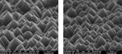
FIGURE 3. SEM image of laser-processed PSG-SE monocrystalline c-Si wafer surface. Left: irradiated with 2.0 J/cm2; right: irradiated with 3.5 J/cm2. Small re-solidified nodules at the pyramid tips can be seen, but otherwise the surface is unchanged. (Courtesy Fraunhofer ISE14)
LFC still appears to be a viable process, though experts acknowledge that the process window has been tight, and some difficulties have arisen due to changing compositions of the dielectric layer. Progress in overcoming these challenges has not been publicly reported in the past 18 months, though insiders believe that the process has been put into pilot-scale production within at least one major PV manufacturer. Against the backdrop of the rapidly-evolving world of advanced c-Si cell processes, the future of LFC looks hopeful but not assured.
Dielectric ablation
As an alternative to creating the rear Al-Si contact after the dielectric passivation is in place, openings in the dielectric layer can be created before the metal is laid down. Lasers have potential to accomplish this task. However, cell performance has been found to be highly dependent on the degree of laser-induced damage to the silicon. For this reason, researchers have generally relied upon the superior ablation results obtained with a picosecond UV laser.9 Today, these lasers are relatively complex and costly. And to obtain the level of process robustness required for volume production, careful design of high-quality laser systems is necessary. Several laser system makers have started down that path.
Similar to the story for LFC, it is too soon to tell whether laser ablation of rear-side dielectric layers will survive the rigors of maturing into commercial volume production. In part, this is due to the fact that, while still a key aspect of the long-term PV roadmap, the introduction of rear-passivated cells has been pushed out by the industry's recent boom times. Tier 1 solar companies' order books have been filled in 2010 and 2011 by demand for solar panels utilizing conventional c-Si cell technology, so the drive to mature advanced cell architectures has slowed. As Finlay Colville, senior analyst with Solarbuzz, stated in mid-2010: "Technologies and c-Si cell concepts considered optional to standard process flows just don't fare well when the industry is growing at a fast rate. Cell makers default to known established production methods that reduce the risk associated with new process flows and equipment types."10
Laser processes for selective emitter formation
One incremental improvement to the standard c-Si process flow has attracted widespread attention in the past two years: selective emitters. As another cell feature that has been studied for decades at the research level, commercial implementation of selective emitter (SE) technology has also been hampered by lack of a fast and low-cost process suitable for mass production. Again, lasers have great potential to fill that need. In cells with selective emitters, the doping level in the emitter region is deliberately varied across the wafer, with areas directly beneath the metal fingers more heavily doped than regions between fingers. This enhances the cell's response to blue light and can significantly increase overall performance. Along with several non-laser techniques, three laser-based processes are now at the evaluation stage.
Laser doped selective emitter (LDSE)
LDSE was developed at the University of New South Wales (Sidney, Australia). In this SE variant, after the SiNx layer has been deposited (FIGURE 1, Step #4), a phosphorous-containing liquid is sprayed or spun onto the wafer's top surface and dried. Next, a tightly-focused laser spot is scanned over the wafer at the locations of the fingers, removing the nitride layer and locally melting the underlying silicon. While the Si is molten, the added phosphorous readily diffuses into the material, increasing the localized dopant concentration. After washing off the residual dopant source, the LDSE process achieves top contact metallization through electroplating rather than conventional screen printing. With the SiNx layer acting as a plating mask, this creates narrow, low-resistivity fingers at the locations where the nitride has been laser stripped, which significantly enhances the performance improvements attained by the SE architecture. Δη values of 2.0 to 2.5% have been routinely achieved in production environments, a very significant enhancement of cell performance.11 Q-switched, quasi-cw, and cw lasers operating at visible (532 nm) and UV (355 nm) wavelengths have all been shown to work in the LDSE process.
This process shows great promise. Due to the large achievable performance gains, LDSE has attracted widespread interest in the industry, and it has been licensed by UNSW to a number of Asian PV manufacturers. Laser tools have been under development by Roth & Rau AG and other laser system makers since 2008. Despite this momentum, however, volume production of LDSE cells appears to be proceeding more slowly than anticipated. Again, this is explained partly by the PV industry's recent market dynamics favoring rapid capacity expansion of conventional process equipment over new tooling for high-efficiency cell concepts. From a technology perspective, though, many PV scientists view the new plating processes with a degree of skepticism, citing significant problems with adhesion of the metal to the silicon. This poses questions about process control and achievable high-volume manufacturing yield – a key issue. It remains to be seen whether this issue poses a serious obstacle to eventual production scale-up.
Liquid chemical processing
Another laser process pioneered by the Fraunhofer ISE (Freiburg), liquid chemical processing (LCP) creates a selective emitter in a manner similar to that of LDSE, in that it uses a laser to simultaneously pattern the SiNx layer while inducing localized dopant diffusion. The main difference is in the delivery mechanism for the phosphorous-containing liquid. Rather than being applied to the entire wafer surface, the liquid is directed at the wafer in the form of a jet that also serves as a light guide to deliver the laser beam. The technology is based on the waterjet-guided laser developed and commercialized by Synova S.A. The process uses either IR or visible (green) q-switched lasers and is sensitive to laser pulsewidth. After doping, metallization can be achieved with either plating techniques or conventional screen printing. It is said that the presence of the liquid reduces laser-induced defects in the silicon that can be created by "dry" laser doping process such as LDSE. Δη values of ~1.0% are claimed.12
LCP process tooling is now under development through a joint venture of Synova and RENA GmbH, a PV equipment company specializing in wet chemistry processes. The complete solution combines the laser equipment and RENA's plating tools. In order to achieve production-viable throughput, multiple waterjet-guided beams must be employed in parallel. A small number of evaluation units have been shipped to date that feature eight nozzles, while designs for full-scale production machines include several dozen jets.
There are no reports of fundamental technical issues with the LCP process. The concept was well established by Fraunhofer ISE before being taken up by RENA, so process risks appear to be minimal. Machine complexity may be a challenge, however, given the multiplicity of jets and the sophisticated nozzles used to form each laser-beam-guiding jet. Following customer evaluations, the decision timeframe for proceeding with productization of full-scale tooling is expected in late 2011 or early 2012.
PSG-based laser doping
A third variant of laser doping for SE formation uses as the dopant source the phosphor silicate glass (PSG) layer formed on the wafer surface in the standard emitter diffusion process (FIGURE 1, Step #2). The laser step is thus moved to near the front end of the process flow. Since no additional dopant gases or liquids are needed and standard screen-printed metallization is retained, only the laser tool is added to the equipment set. The process was developed and championed in the late 2000s by the University of Stuttgart-IPE13 and Δη values of 0.4 to 0.5% are reported.
Owing to the greater width of screen-printed fingers and limitations on placement accuracy of the screen-printing tools, a wider swath must be laser processed for each finger. The laser beam is formed into a line or a rectangular spot typically 200 to 300 micron wide, with a uniform irradiance profile. Currently, first-generation PSG-SE tools are being offered by both Centrotherm Photovoltaics AG and Manz Automation AG, with at least one other well-established laser system vendor considering development of a system. Centrotherm's tool employs a 532 nm q-switched laser with a rectangular spot, requiring laser power in the hundreds of watts. Manz's tool also uses a q-switched 532 nm laser, but its line beam only requires laser power in the tens of watts. While early research by IPE-Stuttgart suggested that melting of the silicon was required, more recently Fraunhofer ISE has found that avoiding melting of all but the tips of the surface-texturing pyramids (on monocrystalline Si wafers) is critical to achieving reasonable Δη values (FIGURE 3). Dr. Peter Fath, Centrotherm's CTO, thus describes his company's PSG-SE process as more of a "turbo-RTP" (rapid thermal processing) effect, re-distributing and activating dopant atoms, than a classic laser doping process.14 Obtaining a highly uniform beam profile at the wafer surface is key to accomplishing the required process control.
Centrotherm has shipped several evaluation units to both Asian and European cell makers. For laser tools retrofitted into an existing manufacturing line, the company promises Δη ≥ 0.3% and during a recent two-month pilot production ramp in China, they achieved 0.42%. As this article goes to press, the first month of a similar production ramp at a German PV manufacturer has yielded 0.25%.
Despite its lower efficiency gain, the PSG-based laser doping process could turn out to be more commercially successful than LDSE or LCP. Since only a single tool is added and the rest of the line is unchanged, the process is relatively easy to add to existing conventional production facilities and the additional capital cost is relatively low. Though still in the early days, it appears that the process is gaining some traction among cell makers not looking to hit a home run with regard to efficiency gains, but still interested in adding a low-cost incremental improvement.
Conclusion
As Solarbuzz's Finlay Colville observes, the past year's booming PV market and "astonishing" rates of capacity expansion in China and Taiwan have pushed out the implementation of advanced cell architectures in high-volume production. Colville notes, "New cell concepts – all of which do have strong laser-based tooling pull – are then confined to R&D labs or low-volume pilot line builds. All this said, however, there is barely a c-Si solar manufacturer who is not considering a laser-based process as an essential part of their technology roadmap...."
Alejandro Becker, sales manager and director at Innolas Systems GmbH, concurs: "Laser processes in PV manufacturing will move forward through the involvement of experienced laser system integrators with deep understanding of cell technology as well as lasers and laser applications, and who can produce robust machines with high throughput, high uptime, and high reliability in the 24×7 industrialized production environment." He adds, "Laser technology will not be used because it is fancy, but for its potential to lower production costs per watt of PV output."
Indeed, cost per watt is the name of the game in PV. Without a doubt, lower cost and higher performance are critical aspects of the industry's near-term maturation. Ultimately, lower production costs will translate to lower costs of installed PV systems, driving the cost per kilowatt-hour of photovoltaic power ever closer to parity with that of today's conventional energy sources.
While laser-based manufacturing techniques have not experienced the rapid uptake hoped for by the laser industry three to four years ago, their potential remains high. And the outlook for eventual adoption of at least one technique remains positive. Centrotherm's Fath sums it up well: "Lasers are old friends in PV, but so far there has been no real breakthrough laser process for c-Si," he says. "At Centrotherm, we believe that the PSG-SE process is just such a breakthrough, and from our early experience in its production ramp, we are optimistic that it will be widely adopted in the industry."
References
- Murison, R., et. al., "CIGS P1, P2, and P3 laser scribing with an innovative fiber laser," Proc. 35th IEEE PV Specialists Conference, 2010.
- Patel, et.al., "Improving throughput and quality of photovoltaic laser scribing," Laser Focus World, Vol. 47, No. 7, July 2011.
- Solarbuzz PV Equipment Quarterly Report, Q4, 2010. Also: personal communication, Finlay Colville, May, 2011.
- Janssen, G, "Laser processes for high efficiency solar cells," Lasers In Silicon Photovoltaics Seminar, Munich, May 25, 2011.
- Schulz-Ruhtemberg, M., "Application of new laser sources," Lasers In Silicon Photovoltaics Seminar, Laser World of Photonics Conference, Munich, May 25, 2011.
- Pantsar, H., "Laser process optimization for improving emitter wrap through drilling rates," Proc. 35th IEEE PV Specialist Conference, 2010.
- Gunther, E., "Applied Materials: back contact photovoltaic revolution," May 8, 2011. http://guntherportfolio.com/2011/05/applied-materials-back-contact-photovoltaic-revolution.
- John, J., et.al., "A Review on 5 years cell development within the European Integrated Project Crystal Clear," Proc. 24th European Photovoltaic Solar Energy Conference, 2009.
- Rana, V., et.al., "Selective removal of dielectric layers using picosecond UV pulses," Proc. SPIE Conference 7193 (2009).
- Colville, F., "Laser processes in solar remain firmly on long-term roadmaps as cell makers in China and Taiwan define short-term equipment trends," Photonics Online, July 26, 2010.
- Tjahjono, B.S., et.al, "18.9% efficient laser doped selective emitter solar cell on industrial grade p-type Czochralski wafer," Proc. 25th European Photovoltaic Solar Energy Conference, 2010.
- Kray, D., et.al., "Industrial LCP selective emitter solar cells with plated contacts," Proc. 35th IEEE PV Specialist Conference, 2010.
- Röder, T., et.al., "0.4% absolute efficiency gain of crystalline silicon solar cells by laser doped selective emitters," Proc. 34th IEEE PV Specialist Conference, 2009.
- Jäger, U., et.al., "Beam shaping - the key to high throughput selective emitter laser processing with a single laser system," Proc. 35th IEEE PV Specialists Conference, 2010.
Corey Dunsky, an expert in laser-based processes and hardware for advanced manufacturing, is the president and founder of Aeos Consulting Inc., a provider of technology, market, and strategy development as well as engineering design services to high-technology equipment and manufacturing companies. Prior to founding Aeos, he held various management and technical positions at Coherent Inc. and Electro Scientific Industries Inc. At Aeos, Dunsky advises clients in the laser, photovoltaics, and other high-tech industries on process and hardware development. He holds a Ph.D. in mechanical engineering from the University of California, Berkeley. He can be reached at [email protected].
Past ILS Issues