Picosecond lasers enable novel marking techniques
DUNDEE, SCOTLAND – The availability of industrialized ultrafast (picosecond and femtosecond) lasers is impacting many fields, including marking. The athermal processing properties of their short pulses often deliver superior results. Several materials can be "cold"-ablated or transformed with higher resolution, and delicate and/or thin materials can be similarly marked with virtually no heat-affected zone. These properties are enabling new marking modalities such as "black marking" for imprinting a high-quality logo on tablets and smartphones. At the University of Dundee, we have developed new types of novel marking methodologies using a Coherent picosecond laser. While these are aesthetically attractive and could be used, for example, for creating logos or even jewelry, we believe that they have broader potential as functional elements in other industries.
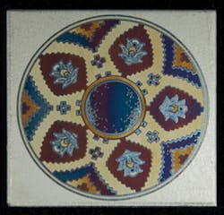
Visually stunning is our color marking on uncoated metal surfaces—FIGURE 1 shows an example of the type of full-color mark we can create. The color effect is actually created by thin-film optical interference. We have discovered that the intense localized energy from a focused picosecond pulse in the presence of ambient air can strip electrons off the metal surface, causing it to react with oxygen and leaving a thin layer of metal oxide. If this layer is on the order of half the wavelength of visible light, then the treated surface will demonstrate a large wavelength bias (color) when it reflects light. In practice, we determine empirically the optimum fluence and other parameters that produce various colors for each type of metal. We can then input these to software we have developed that allows us to automatically create a full-color pattern from a CAD file. Because it relies on intense highly localized energy, we have found that the method yields the largest range of vibrant colors on metals that are poorer thermal conductors, such as titanium and some steels. This particular example on titanium was inspired by a classical Persian carpet pattern. As with black marking, the pattern is integral to the substrate with no surface relief, making it a robust potential option for logos on consumer products, for example.
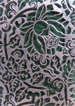
More unusual yet, FIGURE 2 shows our ability to create metal patterns inside transparent glass using the picosecond laser. This marking method also employs some interesting electro-chemistry and takes advantage of the fact that common glass types like soda glass contain metal ions such as sodium. In our process, we first put metal paste (here, silver) on one side of a thin glass substrate. We then heat the glass to moderately elevated temperatures while applying a strong electric voltage across it, with the positive electrode on the silver side. Positive metal ions move towards the negative electrode, so the net result is that native positive ions (mostly sodium) are pulled out of the glass and replaced with metal ions. After cooling, the glass is still transparent and visually unaffected.
When we focus picosecond pulses into this silver-ion doped glass, nonlinear absorption occurs at the focused beam waist. Here, the intense peak electric field creates free electrons that combine with the positively charged silver ions to form silver atoms that cluster into silver particles. The laser pulse parameters and focusing details are used to pre-determine the size and spacing of these metallic nanoparticles. The process can be used to create elaborate, detailed permanent marks, again with no surface relief. More importantly, glass is a nonconducting dielectric increasingly used for substrates and interposers in advanced packaging formats. The ability to produce three-dimensional (3D) conducting metal lines in glass obviously presents exciting new possibilities.
A third new process involves marking inside this glass and involves nanotechnology, but in this case the marks exhibit optical dichroism. This is a term that refers to a material that behaves differently when illuminated by linearly polarized light at different polarization orientations. As shown in FIGURE 3, we can make marks of this type where the dichroism occurs at visible wavelengths, and the polarization of illumination and/or viewing optics thus influences the observed colors of the mark.
For optically dichroic marks, we use a special glass that contains embedded nanospheres of silver with approximate diameter in the 40nm range. The laser naturally outputs linearly polarized light and when this is tightly focused within this type of glass, the high electric field leads to atomic mobility in the particles, which are then reshaped into a cigar-like form along the polarization of the laser beam. (The long axes of the reshaped nanoparticles—ellipsoids—are oriented parallel to the electric field vector of the picosecond beam.)
Like the other new mark types, we believe this optically dichroic marking technique has potential far beyond a first laboratory demonstration like this. Specifically, it could be used to fabricate new types of passive and active telecom components, and even as the basis for enhanced 3D data storage.
This article was provided by Amin Abdolvand ([email protected]), professor and chair of Functional Materials & Photonics at the University of Dundee, and Frank Gäbler, director of marketing at Coherent.


