How laser surfacing relates to laser marking

Process allows manufacturers to laser-mark challenging materials
TONY HOULT
The laser marking industry has grown significantly over several decades to the point that there is now a very large number of laser marking system suppliers worldwide serving almost every industry. The most-important change in this market has been the introduction of low-power pulsed fiber lasers, which has recently progressed to almost every supplier having a fiber laser marker in their range. These lasers typically have wavelengths in the near-infrared (NIR) regime around 1070nm, which makes them highly suitable for marking most metals because of the lower reflectivity of this wavelength when compared to longer-wavelength CO2 lasers.
But even at this wavelength, some metals are easier than others. Aluminum, copper, and their alloys are widely used across almost every industry and can be laser-marked, but obtaining a low-heat, dark mark with high contrast visible to the unaided human eye on these metals can sometimes be challenging. In addition, a technique has been demonstrated showing that highly transmissive materials can also be marked and textured with minimal damage in a pulse-duration regime not normally associated with this unexpected nonlinear behavior.
Laser surfacing processes
Within the broad field of industrial laser materials processing, the term laser surfacing has generally been employed to describe a range of processes that use continuous-wave (CW), multi-kilowatt NIR laser sources. These processes, however, are entirely different from the techniques described in this work, which can be considered as micro- and nanoscale surfacing applications. Many such processes have been developed using short pulse-length pico- (10-12) and femtosecond (10-15) ultrafast lasers, and much has been written concerning the mainly athermal mechanisms by which they can modify surfaces [1].
The major drawback with these processes is that the capital and running costs of even low-average-power lasers of this type are still high. As process speed is generally controlled by the average power of the laser, the cost for laser processing at realistic surface-coverage rates can be too high for the majority of industrial laser users. Recently, the range of well-established pulsed nanosecond fiber lasers has been extended into the sub-nanosecond regime-and along with this has come an order-of-magnitude increase in peak power capability. This has enabled the development of new laser surfacing processes that employ these cost-effective laser sources in a less well-known, long picosecond processing regime.
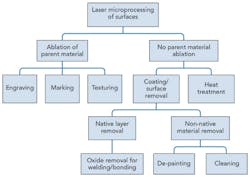
Although these techniques are often referred to as laser texturing [2], mechanistically these processes are related to laser marking, as they are limited to the surface of a component and usually rely on a combination of ablation and melting. FIGURE 1 is an attempt to categorize this very wide range of processes based on a combination of accepted industry terms and the major physical mechanisms involved.
NIR fiber lasers
The widely accepted benefits of fiber lasers ensured that they became the dominant NIR laser source of choice for most of the applications in FIGURE 1. Certainly, the availability of high average power (up to 4kW) from pulsed fiber laser sources is kickstarting laser cleaning and laser de-painting applications [3]. The new fiber laser used here has a pulse-duration range from 0.15 to 5ns, peak power capability up to 0.5MW, high brightness of M2 <2, and repetition rates >1MHz with up to 30W average power. This work aims to improve understanding of the micron-scale features that constitute a laser-textured or -marked surface in the context of marking copper and glass, materials that are usually considered difficult to mark with standard IR wavelengths.
An explanation of the physics of laser processing in this regime is beyond the scope of this article, but clear nonlinear processing behavior is observed. To our knowledge, such behavior was until recently considered the sole preserve of less cost-effective ultrafast lasers.
Analyzing laser texturing and laser marking
A laser mark becomes useful by changing the surface of the laser-marked area in some way to achieve visible contrast with the unmarked area. Some early results were presented [3, 4], but in-depth characterization of laser-textured metal and glass surfaces is presented here using advanced analysis techniques.
A stylus-type surface profilometer is perhaps the best-known and most widely available technique for quantifying the topography of surfaces, so this technique was used here for initial assessment of laser treatments. The morphology of a surface describes the more general features and shapes of surfaces both qualitatively and quantitatively and an imaging technique is more useful here, so 2D and 3D images from a confocal scanning laser microscope were used.
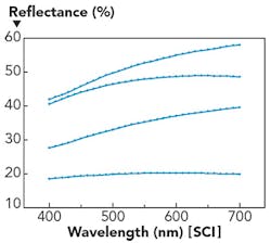
Advanced spectrophotometers [5] are widely used for quantifying the color of a surface. This is achieved by analyzing the light reflected from a surface at many points on the visual spectrum, resulting in a unique reflectance curve for each surface-performed either with or without the specular component included. These instruments are also widely used for measuring the L* value or blackness of a surface, and this technique is now essential for quantifying laser marks on various consumer products. These reflectance curves and L* values are used to quantify the effects of high-peak-power, short-pulse-duration fiber lasers (FIGURE 2) on three challenging material types—aluminum, copper, and glass.
Laser surfacing or texturing of aluminum
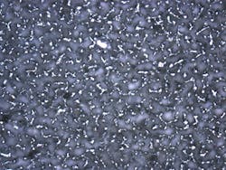
In the case of aluminum, the natural oxide layer is hygroscopic and increases in thickness with time, so simply removing this rough, contaminated oxide layer to expose the underlying aluminum may be enough to create sufficient contrast. An additional complexity is that the degree to which the underlying surface is melted or ablated can significantly affect the appearance of the mark. Careful adjustment of the laser parameters can produce a shinier surface that exhibits more melting to improve contrast. Creating dark, heavily oxidized surfaces on aluminum is readily accomplished by using pulse energy ~1mJ, but achieving low L* values while still producing a robust and non-friable surface so that the appearance of the mark does not change with the observation angle requires careful process control. A darker, more-absorptive surface with a higher L* value can also be produced by increasing ablation to produce a micro-rough surface (FIGURE 3). The surface features shown are all <10μm in size and surface roughness (Ra) is much lower at <5μm.
Removal of anodized coatings from aluminum surfaces is a widely used technique and the same rules with regard to the effect of the laser on the substrate apply—more melting produces more reflective surfaces. In both bare and anodized aluminum, marking speeds are high-on the order of 1–2m/s. Recently, laser marking of certain anodized coatings—albeit at much lower marking speeds than those discussed above—has been developed to the point at which L* values <30 can be achieved using low- and sub-nanosecond fiber lasers.
Laser texturing or marking of copper
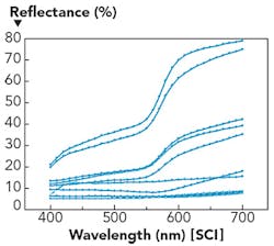
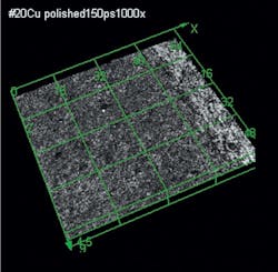
Laser polishing of copper to create contrast is relatively well-known, but producing a black mark is typically more problematic because of the high intrinsic reflectivity of this metal. Techniques have been developed at IPG Photonics Silicon Valley Technology Center (SVTC) to create black surfaces on copper with L* values <30. As seen in FIGURE 5, the difference between the roughness of the laser-treated surface (<1μm Ra) is indistinguishable from the roughness of the prior polished surface. The surface structure, however, is far more complex, with a greatly enhanced surface area. This leads to a highly absorptive surface, as confirmed by FIGURE 4.
The section on the far right of FIGURE 5 is the non-laser-treated, polished area, while the left shows the laser-treated area. These features are an order of magnitude smaller than those produced on aluminum (FIGURE 3). The resultant surface structure supports the hypothesis that a nonlinear, plasma-controlled process rather than a conventional thermal material removal is occurring. Further evidence of this is that the same laser parameters can be used to treat the surface of 20μm-thick copper foil without causing distortion, despite the fact that a sub-nanosecond laser was used at 28.5W average power.
Glass texturing or marking
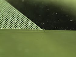
Almost-identical parameters to those used to mark copper can unexpectedly be used for marking both the upper and lower surfaces of uncoated borosilicate glass. This adds weight to the hypothesis that nonlinear absorption is occurring because of the fluence created by the high-peak-power fiber laser. Off-the-shelf laser marking optics were employed, while scan speeds were ~1.5m/s and a standard boustrophedonic scan pattern was employed with a 25μm pitch between lines. Examination of the scribe area showed very limited "crazing," with cracks limited to <10μm and surface roughness of <5μm Ra. FIGURE 6 shows scribe lines and lack of cracking at low magnification.
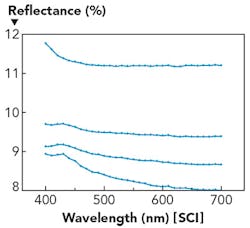
The most interesting result of this process is shown in FIGURE 7, where the reflectance of the glass surface can be closely controlled by changing the scan parameters.
Discussion and summary
We have explored how laser marking and texturing might be quantified, and we have used these techniques on laser marking of aluminum. We have also developed techniques for marking more-challenging copper and uncoated glass surfaces, and it has become clear that there may be other engineering applications for the wide range of surface structures presented.
Laser welding copper to itself or to other metals has always been problematic at low power in the conduction welding regime because of a combination of high intrinsic reflectivity and diffusivity, and inconsistent native surface oxide layers. It has already been shown that this dark marking technique can lead to improved consistency when welding copper. As part of ongoing research, these fine textures have also already enabled improved bonding of either copper or aluminum to other dissimilar metals by improving and normalizing the surface for absorption by the laser beam.
In related work, the same sub-nanosecond laser has been used for a laser pre-treatment process on metals, which can then be subsequently bonded to transmissive polymers. The benefits of a laser-cleaned surface, increased surface area from the laser pre-treatment, and localized laser heating have allowed parent material-strength bonds to be comfortably achieved on certain metal-to-polymer combinations.
Finally, the ability to control the diffusion or light scattering ability of an optical surface to a very fine degree using a conventional laser scanning technique holds promise. Applications being considered are controlling glare, which in turn makes objects more visible to the human eye.
The availability of cost-effective fiber lasers with the greatly enhanced capabilities presented here should enable customers to move laser marking from lower-cost applications into higher value-added marking and texturing applications.
REFERENCES
1. K. C. Phillips, H. H. Gandhi, E. Mazur, and S. K. Sundaram, Adv. Opt. Photon., 7, 684–712 (2015).
2. I. Etsion, J. Tribol. – T ASME, 127, 248–253 (Jan. 2005).
3. T. Hoult, V. Kancharla, and A. Amidon, "Processing of surfaces with kilowatt level nanosecond pulsed fiber lasers," Proc. ICALEO, paper 1402 (Oct. 2015).
4. T. Hoult and A. Amidon, "Laser surface texturing with new fiber lasers," Industrial Laser Solutions, 30, 6, 15–20 (Nov/Dec. 2015).
5. See http://sensing.konicaminolta.us/products/cm-700d-spectrophotometer.
Dr. TONY HOULT([email protected]) is applications manager at IPG Photonics Silicon Valley Technology Center, Santa Clara, CA; www.ipgphotonics.com.