3D printers: Judgment day
Interest in additive manufacturing (3D printing) went viral this year, and with that interest came more confusion on exactly what this technology can do and where it stands in its adoption cycle. Articles in Main Street media describe machines capable of printing homes, jet engines, and even suggest the possibility of "a factory on every desktop," where you can print whatever you want, whenever you want it. This visual is exciting and conjures up images of the replicator and Skynet building new and better Terminators with autonomous 3D printers. But before we start worrying about Judgment Day, it might be worthwhile to take a step back and examine the additive manufacturing (AM) landscape and the variety of technologies, materials, and processes needed to bring that vision to reality.
Involved technologies
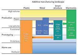
Additive manufacturing encompasses a broad range of technologies that can be used to make devices in plastic, metal, and even electronic materials. The technology used to additively make plastic parts may be quite different than that used for metal or electronics, and there are even variants of a technology for processing a given material based on application requirements (FIGURE 1). For example, AM technologies such as stereolithography (SLA), Fused Deposition Modeling (FDM®), and selective laser sintering (SLS) are available to make parts using plastic materials, such as photopolymers and thermoplastics (PLA, ABS).
In FDM, a plastic filament is unwound from a coil and supplies material to an extrusion nozzle, which can turn the flow on and off. The nozzle is heated to melt the material and is moved in both the horizontal and vertical directions by a motion control mechanism, driven by a tool path created directly from a CAD model (FIGURE 2). In SLS [a.k.a. selective laser melting (SLM) or powder bed], a high power laser is used to selectively melt a bed of plastic powder in a layer-by-layer process to build up the physical part. The end result is buried in the powder cake and is not visible until the excess powder is removed and the part is revealed. The terms SLM and SLS are often used interchangeably to describe this process, although the ASTM F42 standards committee prefers laser sintering, even though it acknowledges this is a misnomer because the process fully melts the material into a solid mass. Each process has its advantages, for example, FDM uses production-grade thermoplastics, which can endure high heat, caustic chemicals, and intense mechanical stresses, whereas SLS produces higher resolution parts and is faster.Similarly for metals, AM technologies, such as SLS (a.k.a. direct metal laser sintering when used for metal parts) and free form fabrication are available. The SLS process for metal is essentially the same as described above, except metal powder is used instead of plastic. However, in free form fabrication, the process simultaneously delivers feedstock material (metal powder or wire), and a heat source (laser or electron beam) builds up the part in free space. The entire process is visible as the part is grown up layer by layer. The heat source creates a small molten pool of metal from the feedstock, which is supplied to the focal point of the heat source through the deposition head. A multi-axis motion control system is used to move the deposition head and/or part to build each layer. In some implementations, either an inert shroud gas or a hermetically sealed chamber filled with inert gas is used to protect the part from atmospheric oxygen and moisture for better control of build properties.
LENS
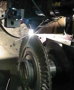
Laser Engineered Net Shaping (LENS®) technology is an example of a free form fabrication process within an atmosphere-controlled chamber that uses powdered metal feedstock and a laser heat source. Each metal processing method has its advantages, for example, the SLS powder bed is better for complex geometries and smaller volume parts, whereas the LENS technology is better for larger volume parts and applications that require high mechanical properties. Also, the LENS process can add materials to an existing part, which enables repair applications (see FIGURE 3). Repairing or re-manufacturing parts with the LENS process provides advantages over repairs made by welding. Because LENS deposition is performed with a small, tightly controlled molten pool of metal, the heat affect zone on the undamaged portion of the component is minimized, reducing distortion. This level of process control with the LENS process also results in repairs with excellent microstructure and properties. And since the process is computer controlled, no operator intervention is required during deposition. The LENS process can also mix multiple powders together during deposition to create parts with blended or graded materials. This feature is useful in speeding the development of new alloys.Printed electronics
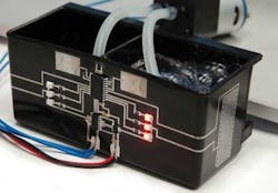
Printed electronics is another emerging AM technology used to print circuits and electronic components. As with plastics and metals, AM for printed electronics is a CAD-driven process that eliminates hard tooling and wasted materials associated with subtractive processes. Initial methods for printing electronics leveraged technologies used by the graphics industry, such as ink jetting, screen printing, and gravure. More recently, new methods, such as Aerosol Jet® printers, have been developed specifically for printing electronics. The Aerosol Jet process first atomizes a liquid electronic material (e.g., conductive metal or polymer inks, dielectrics, and semiconductor materials) into a fine mist, which is delivered to the deposition head. A gas is then introduced through the deposition head, which compresses the mist into a tightly collimated beam that prevents the nozzle from clogging. The beam remains focused from up to 5 mm above the surface and can be used to print electrical features, such as conductors, resistors, capacitors, insulators, sensors, antennas, and even semiconductor components. Different nozzle sizes allows Aerosol Jet systems to print high-resolution features less than 10 microns in width or features up to a centimeter wide in a single pass. Due to the long focal length of the Aerosol Jet beam, these electronic features can be printed on 2D or 3D surfaces (see FIGURE 4).Total process
The AM deposition technologies described above are just part of the total process required to bring these new methods into production for real functional parts. For example, printed plastic or metal parts may require post-processing to remove support materials or improve surface finish. Metal components may need further treatment to improve mechanical performance through processes such as hot isostatic pressing. When printing electronics, the substrate may require treatment prior to deposition to control surface energy, and another treatment after deposition to sinter or cure the electrical material for performance. Although these technologies are radically changing the manufacturing footprint, new considerations and manufacturing skills are required. Thus, it is not as simple as just loading your material, pushing the print button, and voilà.Combining technologies
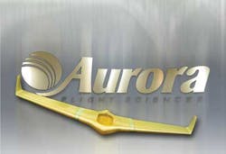
Recent developments have shown the potential of combining various AM technologies to produce highly integrated electro-mechanical devices. Printing electronics onto or even inside the surface of plastic or metal structures can reduce weight, size, and assembly cost, while also increasing performance and reliability for many devices. For example, adding creep sensors to compressor blades used in a gas turbine engine can provide in situ health monitoring of the system. Or printing functional electronics onto complex-shaped structures, such as unmanned air vehicles UAVs, allow them to be built more quickly, with more customization and potentially closer to their field of use (FIGURE 5). The convergence of AM technologies to build these "smart structures" is in its infancy. Today, the processes are serial, but it is not too difficult to imagine an integrated AM machine capable of printing a fully functional smart structure. Many challenges remain, such as process compatibility, surface preparation, material compatibility, and post-processing, just to name a few. Thus, Judgment Day is still a bit off in the future.
