Laser processing enables smaller, faster mobile devices
Micromachining technologies yield high-volume production
HAIBIN ZHANG
At least every two years, when their contracts expire, consumers expect to find exciting, new smartphone models that are faster, lighter, and more attractive than their old mobile devices—and ideally ones that cost less, too. For product designers and engineers, the relentless pace of innovation and ever-rising consumer expectations mean that they must continually explore new manufacturing technologies and processes that improve flexibility, speed, and reliability, as well as lower costs and ensure fast turnaround.
These trends are leading smartphone designers and manufacturers to the micromachining sector of lasers and the laser-based equipment industry. Laser-based systems provide unique capabilities in applications such as drilling, wafer scribing/dicing, material ablation, and surface patterning, which are well suited to high-volume mobile device production. They offer production efficiency and processing quality well beyond limitations imposed by mechanical and chemical alternatives. In many cases, they are the only practical option for implementing a particular design specification.
Laser-based micromachining systems consist of multiple, precisely coordinated subsystems. The laser engine usually is the main cost driver of the overall system price, and can be attributed to a majority of system instabilities and failures. A thorough test of the laser's capabilities is a very important prerequisite for high-performance laser machining systems.
Given the demands of modern mobile device manufacturing, simply integrating a laser and a beam scanner is no longer sufficient. Sophisticated beam shaping and steering components are required to extend capabilities beyond what is offered by basic beams. Multi-component beam shapers, splitters, combiners, acoustic optical modulators and deflectors (AOMs and AODs), diffractive optical elements (DOEs), spatial phase modulators, and the combinations of these make it possible to control the size, timing, and location of incoming laser beams.
From a process perspective, a keen understanding of laser-material interaction is crucial to effective management of thermal, plasma, and debris effects to achieve high-quality, high-throughput micromachining. Key technology competencies include beam delivery, system design, system stability, software, control, automation, and a deep understanding of laser-material interactions.
Now, let's take a closer look at some of the applications where laser micromachining will play an expanded role in mobile device manufacturing.
Strengthened glass machining
Chemically strengthened glass is widely used as exterior protective windows for smartphones, tablets, and touch-screen laptops. Depending on the manufacturing process flow, glass mother sheets (sized up to 150 × 180cm) are machined to individual panels before or after chemical strengthening processes. In the One-Glass-Solution (OGS) flow, the glass sheets are strengthened, patterned with indium tin oxide (ITO), and then separated and machined down to individual panels of various sizes. As the glass trends thinner (for weight) and stronger (for protection), the surface compressive stress and center tension increase dramatically beyond what traditional mechanical cutting solutions can handle due to low yield and high cost.
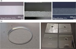
Laser systems, on the other hand, can easily achieve high-quality straight, curvilinear, and internal cuts. For singulation, CO2 lasers, Q-switched nanosecond lasers, and high-peak-power ultrafast lasers are used (FIGURE 1a). High processing speeds of roughly 1 m/s were achieved with excellent edge quality. As a result, high edge strength in the range of 200 to 600MPa (process-dependent) is obtained when measured by four-point bending tests.
PCB patterning: laser direct ablation
The smaller form factor and higher density interconnect requirements found in mobile devices are driving the PCB industry to ever-smaller line widths with much higher density. In leading-edge designs, lines with spacing down to less than 10μm are desired. The traditional "subtractive" PCB manufacturing method, where desired circuit patterns are imaged with lithography and metal films etched to form designed circuitry, can no longer achieve the desired quality and cost due to challenges in throughput, resolution, repeatability, and lack of adhesion.
As a new enabling technology, laser direct ablation (LDA) patterning is a direct-write "semi-additive" method that creates narrow lines down to 5μm width, spacing, and depth. The process employs high-repetition-rate ultrafast lasers and acoustic optical deflectors (AOD) for efficient, high-accuracy material removal and high-speed, precise beam delivery. The substrate is ablated with circuit patterns and copper is plated in the trenches. Depending on the process flow, a follow-up polishing process can help define the circuit with extremely high precision. Because the patterns are embedded, electrical crosstalk is reduced and adhesion is greatly improved.
The LDA system takes advantage of tertiary beam positioning control technology that allows real-time power and beam scanning. A scanning bandwidth of up to 6MHz enables extremely fast patterning—a three-orders-of-magnitude improvement over conventional galvanometer-based scanning techniques. This technology is well-suited to the needs of the mobile market—a cellphone circuit board can be patterned within 20–30s, depending on the circuit density and line width requirements. Line width and depth can be adjusted in real time from 5 to 25μm, which enables a much higher level of integration and saves manufacturing cost.
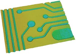
FIGURE 2 illustrates a high-resolution PCB pattern created by such an LDA system for a typical cellphone board pattern and its features. The line width can be tailored down to less than 10μm. A variety of features, including circuit connection wires, vias, landing pads, and isolation areas, can be created with a single scan. The LDA technology enables PCB manufacturers to surpass the line width barrier and gives the circuit designer new tools for patterning due to its fast direct-write capability. This also enables higher-density PCB panels with much less signal distortion and power consumption.
Via drilling for electronic packaging
Via holes are critical features in electronic packaging, where small-diameter holes (140 to >150μm in diameter) are used to connect multiple layers of circuitry. Driven by the need for miniaturization, vias are also shrinking in size in all electronic packaging applications.
For flexible circuits, due to its high absorption by the substrates (mostly polyimide-based), UV laser tools are typically employed. Via sizes from 10 to more than 100μm can be achieved by incorporating various optical shaping technics. Punching with Gaussian or flattop beams, and trepanning or spiral with shaped or Gaussian laser spots are typically used to improve efficiency. In the fast-growing, high-density interconnect (HDI) mobile market, CO2 lasers are often used to create vias due to their unique advantages of low cost and strong absorption by both resin- and glass-reinforced layers. Typical via size ranges from 50 to 150μm, with a recent push from key industry leaders to even smaller diameters. For IC packaging applications, vias with even smaller sizes, some down to 15–20μm in diameter, are desired to satisfy extreme high density interconnect needs.
To enable high throughput while maintaining high quality, yield, accuracy, and repeatability, the latest-generation via drilling systems incorporate AOD scanners in combination with fast galvanometers and linear stages, enabling coordination among AOD, galvo, and large-travel-range linear stages to deliver high-speed machining over large panel sizes. Compared to traditional stitching methods where scan field overlap and feature offsets jeopardize panel integrity, a compound beam positioning system enables continued patterning over large sizes (21 × 25 in.) with high accuracy of <15μm. FIGURE 3 shows vias machined by nanosecond UV lasers on a polyimide substrate and by short-pulse picosecond lasers on ABF materials, respectively.
Summary
Laser microprocessing systems play increasingly important roles in today's electronics industry. In addition, laser additive manufacturing (3D printing), ITO patterning, micro-joining and welding, laser direct imaging (LDI), interposer and through-silicon vias, and high-quality marking are just a few examples of emerging applications, driven by the emergence of new materials and ever-more-demanding mobile device requirements. As the laser processing market grows and matures, laser system solution providers are challenged to compete with competencies not only in lasers, optics, and laser-materials processing knowledge, but also reliable, high-precision beam controlling mechanisms. New generations of intelligent laser solutions will evolve with lasers, photonics, electronics, and automation technologies, and enable the electronics manufacturers to produce the increasingly complex components found in today's mobile devices.
Dr. HAIBIN ZHANG([email protected]) is with ESI, Portland, OR; www.esi.com.


