Laser surface texturing with new fiber lasers
Pulsed fiber lasers have use in new applications
TONY HOULT and ARTHUR AMIDON
Two new fiber lasers with unique processing capabilities have been introduced that add to an existing range of nanosecond fiber lasers. In the first case, the modularity of fiber lasers enables an average power increase into the multi-kilowatt regime. The second laser extends the utility of variable-pulse-duration master oscillator power amplifier (MOPA) fiber lasers by offering shorter pulse lengths into the long picosecond regime at a low cost/watt selling price. Both lasers operate in unexplored irradiance and power regimes and extend the capabilities of current surface preparation, cleaning, and coating removal processes significantly. As well as further reducing reliance on environmentally unfriendly chemical processes, the two fiber lasers enable novel applications such as improving welding of high-reflectivity metals.
Laser surfacing
Laser surfacing usually refers to a range of multi-kilowatt laser processes such as heat treatment, hardening, and cladding, but here we discuss techniques that produce smaller-scale, finer, and shallower features that are usually referred to as laser texturing. We define a textured surface as one that functionalizes surfaces by producing small-scale, shallow features <10μm deep over large surface areas. Processes that meet this definition have been employed for many years by laser engraving cylindrical forms such as anilox and embossing rolls [1], and pixel sizes can be as small as 2μm (FIGURE 1). Laser engraving of molds falls into the same indirect category in that textured surfaces on other non-metallic materials can then be reproduced by using the lasered surface as a master. Other direct laser texturing applications, such as improving the tribological properties of surfaces, have been researched extensively [2].
However, the improved reliability, flexibility, and cost-effectiveness of pulsed nanosecond fiber lasers, along with the availability of higher average power and higher coverage rates, has already led to an increase in closely related laser surface modification techniques such as cleaning, de-painting, and pre-treating for welding [3-5]. Increasing concern over the use of aggressive chemical treatments is favoring the adoption of laser technology, and the two fiber laser tools are accelerating this trend. It is now possible to generate a much wider range of sub-micron and macro surface features or topographies on a diverse set of materials. There is phenomenologically a clear overlap between laser micromachining, laser marking, laser cleaning, laser polishing, and the focus here—laser surface texturing—so our discussion is relevant to all of these topics.
Introduction to laser surface texturing
To engineers, surface finish and surface texture are terms that are often used interchangeably to describe surfaces obtained after the completion of manufacturing processes. To illustrate the three major characteristics of surfaces, a sand dune analogy may be useful (FIGURE 2).
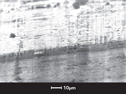
Clusters of sand grains represent surface texture or surface finish, while waviness is the ripples in the sand and curvature or form is the undulating nature of the sand dune. As laser beam processing is non-contact, workpieces are not subject to the forces imparted by mechanical machining. So, controlling waviness and curvature is no longer a mechanical issue, but becomes a question of controlling the motion of the zero-mass laser beam. Most laser surface texturing applications require covering large surface areas at high speed and, hence, the focused laser beam will typically be moved boustrophedonically (relating to writing alternate lines in opposite directions) at high speed over the surface using a galvanometer scanner. This technique can impart changes in the waviness of a surface. FIGURE 3 is an example of how a small change in waviness is imparted to the surface by adjusting laser and motion parameters to increase material removal, and much larger changes can also be realized.
If true 3D shapes with significant curvature in addition to waviness are required, multi-axis laser systems can achieve this for parts using either subtractive (laser micromachining) or laser additive manufacturing (LAM) techniques. However, controlling surface roughness (Ra) down to low levels is a more complex issue, especially if high coverage rates are needed to make laser texturing relevant for large-scale industrial manufacturing.
Controlling texture with lasers
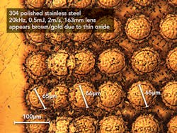
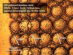
Pulsed nanosecond fiber laser marking is a form of laser texturing. Ablative laser marks appear highly precise to the unaided human eye because of their small feature size, but FIGURE 4 shows a typical laser mark on stainless steel under magnification. Rapid melting and a highly dynamic reactive, vapor-pressure-induced ejection of molten material occurs at high laser irradiance. Subsequent re-solidification leads to highly randomized surface features. This complex surface makes a simple Ra measurement an oversimplification and of limited usefulness for checking mark quality—the main criterion for which is usually a subjective assessment of readability to the unaided eye.
Specialized techniques are available to improve surface finish on laser-marked and laser-micromachined features. Multiple laser passes, a wide variety of scan patterns, and on-the-fly laser and process parameter changes are all used to achieve the required Ra. Very high-peak-power, short-pulse ultrafast lasers are used for micromachining and these lasers may produce less collateral heating and less melting, but their cost per watt are high. Low material removal rates per pulse typically lead to lower Ra, but these lasers are limited to specialized applications where high precision and demanding cosmetics are paramount. Highly sophisticated, multi-axis laser machines extend these subtractive techniques into the manufacture of complex, high-precision 3D components by subtractive laser ablation [6]. However, the basic difference between mechanical and laser machining is a focused energy point source such as a laser beam, which makes this final step challenging. At this point, it should be noted that for many applications, a smooth surface is not required. For example, the micro-rough nature of the surface in FIGURE 4 makes the mark more visible to the untrained eye. The new laser developments presented here show that a range of surface topographies can be produced to suit a particular requirement and the surfaces can be functionalized.
Kilowatt-level pulsed nanosecond fiber lasers
The first of these lasers is a significant extension of a well-known range of Q-switched fiber lasers. The modular nature of continuous-wave (CW) fiber lasers allows scaling to unprecedented average power [8]. Similar modularity now allows scaling of pulsed nanosecond lasers up to multi-kilowatts (FIGURE 5), as higher average power increases process speeds up to those that are necessary to justify adoption of these techniques by industry.
Major applications for high-power pulsed nanosecond infrared (IR) lasers are de-painting, removal of aluminized coatings from steel, and pre-joining surface treatment of aluminum [8, 9], and coating removal rates of up to 60cm2/min have been reported [10]. Fiber lasers offer superior average power and pulse energy in a smaller footprint. To compare, a nanosecond-pulse-duration diode-pumped solid-state (DPSS) laser with only 800W average power has 10X larger volume and 3X larger footprint, as well as higher capital expenditure (capex), service, and running costs.
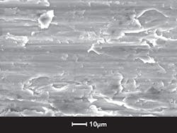
Thick native oxide layers on aluminum are known to be deleterious to most joining processes, and removing these layers improves both adhesive bond performance and weld quality. FIGURE 6 shows the poor surface condition of an untreated mill-finish 1100 series aluminum alloy at high magnification. It is easy to understand that the unevenness of this surface leads to a highly variable thickness and condition of the native oxide layer, leading to poorly repeatable surface properties. Stimulated by increasing interest from the transport industry in aluminum alloys for weight reduction, our trials evaluated the performance of this high-power fiber laser for a range of possible aluminum surface textures.
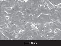
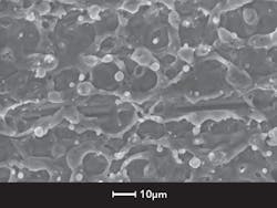
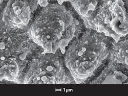
The phenomena observed range from simply cleaning or normalizing the surface (FIGURE 7) to melting and melting and removing significant amounts of material from surfaces (FIGURE 8). Extending average laser power has allowed faster processing up to the point at which these processes have now become economically viable in terms of both capex and running costs.
Improving adhesive bonding
The increased use of adhesive bonding for light weighting in the automotive industry presents an important opportunity for this process. It has been shown that high-average-power nanosecond laser treatment leads to improved adhesive bond strength by:
- Increasing surface energy;
- Removing contaminated hydrated oxide layers that lead to long-term bond degradation;
- Improving surface consistency; and
- Improving mechanical interlocking of the adhesive to the surface because of the significantly increased surface area.
Ultrafast sub-nanosecond fiber lasers
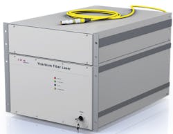
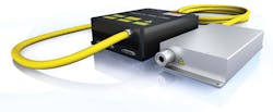
The laser shown below is a development of an existing range of low-nanosecond MOPA fiber lasers. In this case, a semiconductor seed laser runs in gain-switched mode to produce sub-nanosecond pulses. The resulting laser is compact and cost-effective (FIGURE 9).
Available average power is 30W at 150ps pulse duration, and the platform will scale to 100W average power. Its 400kW peak power and high-brightness M2 <1.3 leads to huge irradiances on the workpiece using off-the-shelf optics. Although similar and greater irradiances are achieved using costly, low-picosecond lasers, the 150ps regime is not widely studied.
Our experiments reveal very finely textured surfaces on a range of metals. Copper and aluminum were chosen, as both are difficult to laser machine, their reflectances are close to 100% at room temperature, and their thermal diffusivity is typically 5X that of steel. Highly absorptive, smooth, non-friable dark marks are produced on these metals at coverage rates <10mm2/s. Of particular interest is that metal foils as thin as 50μm can also be marked distortion-free.
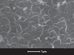
The maximum peak-to-peak height, Rt, of the surface shown in FIGURE 10 is approximately 0.6μm. This is slightly greater than the as-rolled waviness of the surface, confirming that a very fine re-distribution of the surface has occurred. Modern contact angle measurement techniques are widely accepted as providing an accurate quantification of degree of cleanliness and by association, wettability and surface energy. There is also a well-known relationship that confirms a decrease of contact angle with time that is related to rebuilding of the native oxide layer on the surfaces of these metals [9]. For both aluminum and copper, a reduction of >30% in contact angle was measured 24 hours after laser processing with the 150ps laser, suggesting far lower contact angles would be seen shortly after laser processing. The measured reduction in contact angle and related increase in surface energy confirms an important increase in the hydrophilic nature of these surfaces.
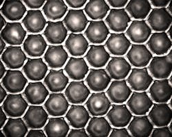
It should be noted that the surface features shown inFIGURES 8and 10 generally resemble each other in shape, but differ completely in scale—FIGURE 8 is at 1000X and FIGURE 10 is at 20,000X.
Welding of high-reflectivity metals
The most important property imparted to high-reflectivity metals by the 150ps texturing technique is the absorptance—these are black surfaces. This is also a permanent, durable, and cleanable mark that is smooth on a macro scale and hence does not trap or fill with debris on handling. This means that all wavelengths of light are strongly absorbed. This is in contrast to an untreated surface (such as that shown in FIGURE 6) where not only is the surface highly reflective, but is also uneven and has a variable oxide thickness. This unevenness is known to contribute to poor spot weld repeatability. Our pre-treatment provides the following benefits when welding:
- More repeatable spot welding of high-reflectivity metals;
- Low-heat-input, repeatable welding of thin, high-reflectivity metal foils;
- Improved weld depth control when welding dissimilar metals;
- Treated areas as small as 1mm in diameter enhances the surface absorption sufficiently for subsequent welding; and
- The same optical train can be used for both the 150ps laser and a near-IR welding laser such as the YLR 150/1500 quasi-CW laser. In this case, a pre-treatment is possible immediately prior to the spot welding process.
We aim to show in future work that this technique is a more cost-effective solution than using high-average-power 532nm lasers or lasers that combine IR and 532nm wavelengths for welding high-reflectivity metals.
Summary
We show here that not only can surface topography be controlled and Ra reduced by lasers, but additional functional characteristics can be produced. The texturing processes presented are normalizing or surface preparation processes that improve the consistency of subsequent processing, laser or otherwise. These processes will improve the controllability of any subsequent processing such as adhesive bonding or welding. Important environmental benefits may be gained by substituting these processes for wet chemical surface preparation techniques.
The essential modularity and scalability of fiber lasers is widening the available range of lasers. We have seen that these new lasers are opening up new applications and commercial opportunities. The two lasers presented here complement each other: high coverage rate but relatively rough surfaces may be produced on metals using a kilowatt-range nanosecond fiber laser, whereas a lower-power, shorter-pulse duration laser may be used to produce very smooth, highly absorptive surfaces on high-reflectivity materials.
These lasers will reduce both capex and running costs to the point at which these processes can become far more widely accepted in industry.
REFERENCES
1. See http://bit.ly/1OS6qeI.
2. I. Etsion, "State of the art in laser surface texturing," J. Tribol. – T ASME, 127, 1, 248–253 (Feb. 7, 2005).
3. See http://bit.ly/1KBlRm0.
4. See http://bit.ly/1Ptmhyj.
5. See http://bit.ly/1LO7PgY.
6. See http://bit.ly/1DmVK4h.
7. J. Wallace, "100 kW fiber laser, power meter serve industry," Laser Focus World, 49, 12, 13–14 (Dec. 2013).
8. See http://bit.ly/1G2VMdM.
9. R. Rechner, I. Jansen, and E. J. Beyer, "Optimization of the aluminum oxide properties for adhesive bonding by laser surface pretreatment," J. Laser Appl., 24, 032002 (2012).
10. V. Kancharla, A. Amidon, and T. Hoult, "Processing of surfaces with kilowatt level nanosecond pulsed fiber lasers," ICALEO 2015, Atlanta, GA (Oct. 2015).
11. See http://bit.ly/1Kt0d59.
Dr. TONY HOULT([email protected]) is the applications manager for IPG Photonics at the Technology Center in Santa Clara, CA, as well as an editorial advisor to Industrial Laser Solutions and a frequent contributor on fiber laser technology, while ARTHUR AMIDON is an associate engineer at IPG Photonics, Oxford, MA, www.ipgphotonics.com.
