Picosecond laser processing of high-tech devices
Picosecond pulses scribe and cut thin, delicate materials with high precision
Colin Moorhouse
The demand to reduce the size, weight, and material cost of leading-edge electronic devices has resulted in a fast-growing requirement for precision micromachining in several industries. Examples include making smaller and more powerful smartphones with brighter displays; reducing the cost and increasing the efficiency of solar cells; and machining bio-absorbable medical stents. The unrelenting pace of innovation in high-tech industries has led to ultrafast (picosecond) industrial lasers, which have become important tools for applications requiring particularly high precision. This is due to the unique operating regime (megawatts of peak power) of this type of laser, enabling clean cutting and patterning of sensitive materials and thin films used in a number of novel devices and micromachining of wide bandgap, "difficult" materials such as glass. In several instances, the picosecond laser is replacing multistep photolithography with a single-step, direct-write laser process. In other applications, it supplants traditional cutting/drilling processes, eliminating the use of chemicals.
Patterning OLEDs
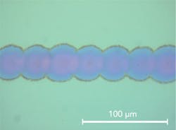
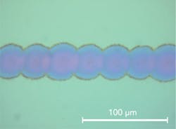
Organic, flexible, electronic devices have many intrinsic advantages including their light weight, thin dimensions, and transparency. In particular, flexible organic light emitting diodes (OLEDs) have tremendous potential for displays since these consume less power than other displays that use backlighting, as well as for general lighting, and can be manufactured on reel-to-reel production lines [1, 2, 4]. A key OLED manufacturing step is scribing the light emitting polymer (LEP) layer. Here, picosecond lasers can readily deliver debris-free patterning and selective depth control because material removal occurs before the material can respond to the acoustic/thermal stress, basically the target material is vaporized before heat can spread from the target area to surrounding material [3]. The superior pulse-to-pulse stability (<2%) of a laser such as the Coherent Talisker is particularly advantageous for fine control of the pulse energy to make consistent scribes; there is no melt or debris on the surface requiring post-laser cleaning. The high laser repetition rate of 200 kHz allows a fast scribing speed of 6 m/s, scalable to 15 m/s using the latest ultraviolet 500 kHz, Talisker 500, as shown in FIGURE 1.
Silicon solar cells
Solar cell manufacturers are striving to reach cost parity with grid power in two ways: (i) reducing cell cost and (ii) improving cell light conversion efficiency. The majority of solar cells are currently based on silicon wafers, and one way to increase the efficiency of these crystalline silicon (c-Si) solar cells is to use a backside passivation layer to reduce recombination losses. In order to make electrical contacts to the cell, holes must be drilled through the passivation layer (typically formed from silicon dioxide/silicon nitride). This must be accomplished with minimal damage to the underlying crystalline silicon to maintain the cell performance and ensure good ohmic contact for current collection. Picosecond lasers offer a lower cost, direct-write alternative to photolithography for this task, eliminating bulk chemical use. Specifically, studies have found that 355 nm picosecond pulses offer selective removal of the dielectric layers with little or no damage to the underlying silicon, allowing the formation of high efficiency solar cells based on selective emitters [5].
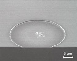
As an example, FIGURE 2 shows the exposed silicon surface following selective removal of a 100 nm SiO2 passivation layer from silicon using 355 nm picosecond pulses. Importantly, there are no melt features in the silicon, as can be found with nanosecond laser processing, thus eliminating the requirement for post-laser chemical etch treatments. In addition, no subsurface damage is visible. Some small particles in the center remain from the ablated dielectric layer, but these can be removed easily by air pressure.
Bioabsorbable stent cutting
Over half a million stents per year are used in the US alone to prop open blood vessels. One complication of early, all-metal stents was restenosis, where plaques form on the stent, re-blocking the opened blood vessel. In response, stent manufacturers developed a second generation of stents that were coated with a bioabsorbable plastic containing an anti-restenosis drug. As the coating dissolves over months, this drug slowly elutes on-site. However, since there are still potential long-term, post-operative complications with these stents, bioabsorbable materials have been developed that disappear completely after providing a support framework over the critical months after vessel opening.
The polymers used in these stents must be strong enough to withstand physical stresses within the body, and there are already many types of bioabsorbable materials that meet this criterion [6]. Extremely high precision (<20 μm) is obviously required to manufacture the stent structure and deliver the requisite smooth surface finish, making the laser an obvious choice for this task. The improved optical absorption available at deep UV wavelengths means that excimer lasers have been a frequent choice for micromachining polymers. An emerging alternative approach is to use UV (355 nm) picosecond pulses focused to a small spot size (~10 μm), which facilitates higher optical absorption in a small localized area. FIGURE 3 illustrates high-quality cuts have been made in poly (L-lactic acid) material (PLLA) using 355 nm picosecond pulses.
Laser drilling of transparent materials
The strength, chemical inertness, and high transparency of glass are the reasons for its wide use in many consumer electronics, such as touchscreens, handheld devices (tablets, smart phones, etc.), and flat panel TVs. Also, future devices are anticipated to rely more heavily on glass to provide additional structural rigidity and to incorporate feature holes that need to be drilled through the glass. But, as glass substrates get thinner to support smaller and lighter devices, traditional glass drilling techniques struggle to maintain the quality demanded. In particular, it is critical that edge cracking and residual edge stress are avoided in touchscreens where the panels almost always break from the edge, even when stress is applied to the center. The high peak power of picosecond lasers can avoid this problem.
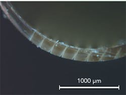
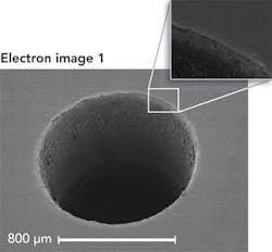
Since glass is essentially transparent to visible wavelengths, either infrared or ultraviolet wavelengths are used. The highest average processing power for maximum removal rates is offered by 1064 nm, whereas the UV wavelength is better suited for thinner glass panels. For example, FIGURE 4 shows high quality, 1 mm diam. holes drilled in 1 mm thick D236T glass using 1064 nm picosecond pulses. There are no microcracks on the edges or sidewalls preventing fractures, ideal for handheld devices.
Summary
Lasers such as the Coherent Talisker have been proven as industrially robust tools, offering sturdy and reliable performance suitable for a wide range of industrial applications even beyond those described here. And the latest UV Talisker 500 is particularly advantageous for precise, small feature sizes in transparent glasses. The combination of short picosecond pulses, excellent pulse-to-pulse stability and high repetition rates delivers precision cuts and patterns with sharp, clean edges and often without post-process cleaning. As a result, picosecond lasers are gaining market share in emerging applications as an alternative to existing laser and non-laser processes.
References
1. T. R. Hebner et al., "Ink-jet printing of doped polymers for organic light emitting devices," Applied Physics Letters 72(5), 519-521 (1998).
2. G. E. Jabbour et al., "Screen printing for the fabrication of organic light emitting devices," IEEE J. Sel. Top. Quantum Electron. 7(5), 769-773 (2001).
3. D. M. Karnakis et al., "Ultrafast laser patterning of OLEDs on flexible substrate for solid-state lighting," J. Laser Micro/Nanoengineering 4, 218-223 (2009).
4. www.fast2light.org
5. V. Rana and Z. Zhang, "Selective removal of dielectric layers using picosecond UV pulses," Proc. SPIE 719321 (2009).
6. P. Törmala et al., "Bioabsorbable polymers: materials technology and surgical applications," Proc. Inst. Mech. Eng., H: J. Eng. Med., 212, 101-111, (1998).
Colin Moorhouse ([email protected]) is with Coherent Inc. (www.coherent.com).
