Selective laser-induced etching enables 3D machining of transparent materials
Process yields high precision without material stresses
MARTIN HERMANS, JENS GOTTMANN, and JÜRGEN ORTMANN
Selective laser-induced etching (SLE) is a new laser technology for rapidly manufacturing true 3D high-precision devices made from transparent material such as fused silica, ultralow expansion glass (ULE), or sapphire. With SLE, parts can be produced that consist of cavities, tunnels, arbitrary undercuts, and even mounted moving parts (FIGURE 1).
SLE: a two-step process
In a first step, ultrafast laser radiation is focused to micrometer-sized spots into a material that is transparent to the wavelength of the laser radiation used. The laser radiation is absorbed, only at the focal spot, by the material because of nonlinear absorption processes occurring at the high intensities that are applied (>1012W/cm2). The absorbed energy leads to internal heating and subsequent quenching of the material in a very confined volume, resulting in a permanent modification of the transparent material. This laser modification does not consist of cracks and can be applied with extreme precision.
This should not be confused with laser-produced 3D pictures in glass that are widely available, although there are some similarities. Line by line and layer by layer, a complete 3D connected volume is exposed inside the glass by 3D scanning of the focus.
Then, in the second step, the workpiece is taken off the laser machine and placed into an etching bath, where only the modified material is dissolved in the fluid etching chemical. The etching starts at the surface and works its way into the workpiece, washing out all the material that was previously modified with the laser radiation.
The high precision of SLE technology comes from extraordinarily high selectivity, as the acronym suggests-selectivity is the ratio of the etching rates of modified material vs. untreated material. For example, the selectivity found in fused silica is larger than 1000:1, resulting in long, fine channels with small conicity coming from one single line of laser irradiation with subsequent etching. Other transparent materials showing elevated selectivities during the SLE process are, for example, Borofloat33, sapphire, ULE, or soda lime glasses. High selectivity is the basis for more complex 3D structures, as they are produced by stacking lines of laser-induced modification next to and on top of each other.
Advantages of SLE are the high precision that is possible (±1μm), no remaining stresses in the material after etching, and true 3D capability. Because of the several analogies to 3D printing, SLE technology can be considered as 3D printing for transparent materials, with the difference being that it works subtractively. Contrary to additive 3D printing, there is no need for supporting structures that must be removed afterwards.
In the SLE process, the remaining glass or crystal is the original one from the datasheets with all the known specifications, as the changed glass material is removed by wet-chemical etching. The advantage arising from this is that there is no need for new certification of materials that are already certified for their specific application. Although SLE surfaces feature an initial roughness on the order of Ra ~200nm, the surfaces do not have microcracks or sub-surface defects that cause failure in cases of mechanical load. This makes applications in the field of flexure bearings possible.
The current state of the technology in fused silica is that first-time-right machining is possible for complex 3D parts <7mm in height with a precision of about 10μm and a maximum tunnel length of 10mm. Larger precision or longer tunnel lengths are feasible, but often make iterations of production and measurements necessary before the part fits the precision requirements.
SLE capabilities
SLE has been demonstrated as a manufacturing technology for fused-silica parts used in various fields of technology with many different applications—not only for prototypes, but also for series production of devices and structures.
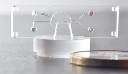
Coupling chips for capillary electrophoresis have been produced (FIGURE 2) in a hexagonal glass part measuring 15mm in diameter, which allows plugging capillaries together without a detectable dead-volume for use in chemical analytics. A light-actuated cell sorter for quicker antibiotic resistance tests with complex 3D microchannels (FIGURE 3) with 34 × 12 × 2mm chip dimensions is useful in biomedical technology and production of food and detergents. New types of 3D nozzles find application in various markets, such as for fuel injection or even inhalers that help with pulmonary diseases. A hollow-cone spray nozzle—for example, producing a spin to the spray—makes a more stable combustion (FIGURE 4) with a 2m height and 60μm nozzle diameter possible.
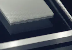
Many ultraprecise micro-sized holes, not necessarily circular in shape, can be drilled into thin glasses or sapphire for semiconductor or electronics applications, such as thin glass vias (TGVs) or holes in display glasses. Hole fields with 2500 150μm-diameter holes, with some having pitches down to 10μm with standard diameter deviations <0.5μm, are possible (FIGURE 5).
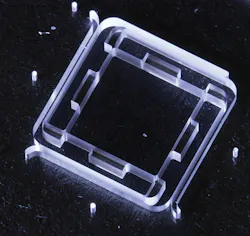
Monolithic MEMS devices can clamp an optical fiber with a flexure bearing or act as a sensor for inertia. Flexures can be cut as thin as 10–20μm that still feature good mechanical stability because no surface or subsurface damages or remaining stresses are induced into the material. FIGURE 6 shows a precision cut from a 1mm fused-silica wafer with a flexure width of 30μm.
Complex 3D precision parts are enabled by the fast LightFab 3D Printer together with an innovative CAD/CAM/NC software chain for digital production, including adaptive slicing and variable filling strategies. The further increase of the precision of the 3D glass parts was achieved using curved vectors automatically generated from 3D CAD data, avoiding the polygonization errors from, for example, stereolithography files. Next to the 3D design, the outline of the chip, including precise structures for alignment, was also produced in the same processing step, reducing the need for post-processing or further precision alignments. After etching and cleaning, such 3D precision glass parts are ready to use.
When a promising design is identified during prototyping and a customer wants it to be fabricated in larger series or even mass production, SLE technology offers the possibility of upscaling to large quantities. So far, the only limit in terms of productivity is how fast the focal spot can be moved through the material. Thus, higher productivity has been demonstrated by accelerating the scan speed.
With the design and integration of specialized fast beam-deflection modules that are tailored to the part to be fabricated, an upscaling is possible and offers the unique possibility of a rapid prototyping technology that can go to mass production. So, 3D printing of glass precision parts is no longer a niche application for only prototypes.
Ongoing developments involve hybrid processes where, for example, two-photon-polymerized structures are created inside of SLE-fabricated microfluidic channels coming from the same machine. Laser polishing can be applied to surfaces that have been machined with SLE to pave the way for future production of complex shaped optics (such as freeform optics, aspheres, and axicons).
MARTIN HERMANS([email protected]), JENS GOTTMANN, and JÜRGEN ORTMANN are all with LightFab, Aachen, Germany; www.lightfab.de.
More Industrial Laser Solutions Current Issue Articles
More Industrial Laser Solutions Archives Issue Articles


