Industrial femtosecond laser applications
Cutting-edge applications include surface nano-periodic structuring, display glass dicing, and dual wavelength femtosecond laser materials processing
Masanao Kamata, Tetsumi Sumiyoshi, Hitoshi Sekita
After extensive research (by many research groups) on the interaction between intense femtosecond laser pulses and materials conducted since the invention of the chirped pulse amplification in 1985,1 high-precision materials processing using femtosecond lasers is now finding innovative opportunities in industry. Compared to conventional lasers, femtosecond laser materials processing can significantly reduce the thermal effect to target materials.2 This is because femtosecond laser pulses can deposit energy into a target material faster than the electron-photon coupling time and therefore the energy diffusion to the surrounding medium does not take place before the affected material ejection starts.
In addition, the high peak intensity of focused femtosecond laser pulses allows micromachining on the surface as well as inside of transparent materials.3,4 With these advantages over conventional laser processing, a wide variety of applications have opened up for femtosecond lasers.
Surface nano-periodic structuring
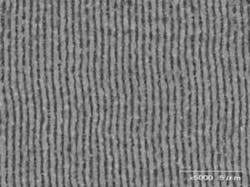
Surface nano-periodic structuring with femtosecond lasers has recently been shown to have positive effects on functionalizing a material’s surface.5 By irradiating the material with femtosecond laser pulses, nano-periodic structures that have a sub-micron periodicity can be automatically formed in a self-organized manner. Figure 1 shows such a structure on a silicon wafer, and these structures can also be fabricated on metals, ceramic materials, semiconductors, and glasses. Major applications of this technique are: a reduction of friction loss on precision sliding parts including automobile engine components, an improvement in adhesion of coating films, and a prevention of attachment of particles and control wettability. Canon Machinery (www.canon-machinery.co.jp) is manufacturing and selling a femtosecond laser surface treatment system, Surfbeat R, that integrates a Cyber Laser IFIRT industrial femtosecond laser.
Flat panel display dicing
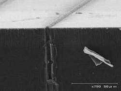
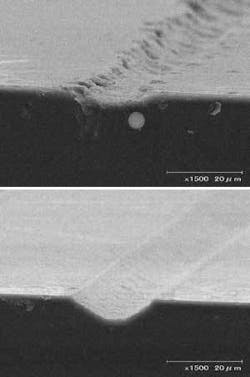
A high-speed and high-quality laser technique is required for glass dicing of next-generation flat panel displays because it is difficult to improve the process yield using conventional diamond blade dicing techniques. For this novel glass dicing technique, femtosecond laser pulses are focused to the rear surface of the glass substrate to make a scribe line (see Figure 2). Because of the ultrashort pulse width, the laser pulses are absorbed by a spatially localized nonlinear ionization and therefore it is possible to process the rear surface of a glass substrate without damaging the front surface. The focused femtosecond laser pulses around the rear surface create cavities6 inside the glass substrate that reach the rear surface (see Figure 3). By ordering this cavity along the scribe line, the glass substrate can be easily broken by mechanical stress or thermal shock.
High-speed glass dicing over 400 mm/s has been successfully demonstrated on non-alkali glass and borosilicate glass, using a newly developed 50kHz, 5W high-power femtosecond laser. This technique can also be applied to the dicing of double layered glass substrates.
Dual wavelength materials processing
For micromachining of transparent materials, deep-ultraviolet (DUV) femtosecond lasers are advantageous over near-infrared (NIR) femtosecond lasers because many transparent materials have strong absorption at the DUV wavelength and also the ultra-short pulse width of femtosecond lasers can avoid unwanted thermal effects. However, the poor conversion efficiency of DUV femtosecond lasers from the fundamental wavelength limits processing speeds. A dual-wavelength femtosecond laser technique has been developed to overcome this drawback. The technique involves using double-pulse femtosecond laser pulses that consist of a pre-DUV 260nm pulse followed by main-NIR 780nm pulses, which improves both the ablation efficiency and the ablation quality.7 The role of the pre-260nm pulses is to create electron-hole plasma to enhance the absorption of the following main-NIR 780nm laser pulses and to decrease the transmission of the 780nm pulses that go beyond the interaction volume.
Figure 4 shows grooves on borosilicate glass surface machined by NIR femtosecond laser pulses and dual wavelength femtosecond laser pulses. Surface micro-cracks and sub-surface damages can be observed for the 780nm NIR femtosecond laser ablation (see Figure 4a). On the other hand, in the case of the dual-wavelength femtosecond laser ablation, the ablation quality and efficiency can be dramatically improved (see Figure 4b). In this case the time delay between pre-260nm DUV pulses and main-780nm NIR pulses was adjusted to 0 ps. The optimum delay time between pre-DUV pulses and main-NIR pulses is determined by complex interplay between energy deposition and dissipation, and therefore it is material dependent. The ablation volume can be enhanced by a factor of 10 when compared to using only NIR femtosecond laser pulses.
In the case of Figure 4, linear absorption and two photon absorption are responsible for the energy deposition of pre-260nm DUV pulses and main-780nm NIR pulses, respectively. This technique can be applied to wider band gap materials because 260nm pulses are nonlinearly absorbed.
Until now, the quality and efficiency of near-infrared femtosecond laser ablation of transparent materials was a trade-off, but the dual wavelength femtosecond laser technique can improve both of them at the same time. This novel femtosecond laser ablation technique is currently applied to trimming thin insulating layers from substrate materials and micro-fluidic device fabrication where a high throughput and high-quality machining is important.
Femtosecond laser solution
In 2004, a Cyber Laser IFIRT femtosecond laser (180 fs, 1 mJ, 1 kHz) demonstrated more than 10,000 hours of maintenance-free operation.8 To ensure a further stability, an APMS (Automatic Power Management System) that enables automatic maintenance of the laser output9 is employed. This laser can maintain a constant laser output under environmental changes such as temperature and humidity. For applications where higher throughput is required a high-power 50kHz, 5W femtosecond laser is available. Michigan University Patent No.3283265 can be licensed to IFRIT users.
Masanao Kamata, Tetsumi Sumiyoshi and Hitoshi Sekita are all with Cyber Laser Inc. in Tokyo, Japan (www.cyber-laser.com).
References
- D. Strickland and G. Mourou, “Compression of amplified chirped optical pulses,” Opt. Commun, 55, 447 (1985).
- S. Nolte, C. Momma, H. Jacobs, and A. Tunnerman, B. N. Chichkov, B. Wellegehausen, and H. Welling, “Ablation of metals by ultrashort laser pulses,” J. Opt. Soc. Am. B 14, 2716 (1997).
- K. M. Davis, K. Miura, N. Sugimoto, and K. Hirao, “Writing waveguides in glass with a femtosecond laser,” Opt. Lett. 21, 1729 (1996).
- E. N. Glezer, M. Milosavljevic, L. Huang, R. J. Finlay, T.-H. Her, J. P. Callen, and E. Mazur, “Three-dimensional optical storage inside transparent materials,” Opt. Lett, 21, 2023 (1996).
- H. Sawada, “Application of periodic structures produced with a femtosecond laser,” Rev. of Laser Eng. 33, 525-529 (2005).
- E. Toratani, M. Kamata, and M. Obara, “Self-fabrication of void array in fused silica by femtosecond laser processing,” Appl. Phys. Lett. 87, 171103 (2005).
- M. Kamata, S. Tsujikawa, T. Sumiyoshi, and H. Sekita, “Dual wavelength femtosecond laser materials processing,” CLEO 2007 technical digest CThM3, Baltimore, MD (2007).
- K.Takasago, T.Imahoko, N.Nakata, T.Sumiyoshi, and H.Sekita, “10,000-hour maintenance-free operation of 1-W femtosecond laser for industrial applications,” Proceedings of the Pacific Rim Conference on Lasers and Electro-Optics 2005, CFE1-5.
- K. Takasago, T. Sumiyoshi, N. Nakata, and T. Imahoko, “Auto power management system for femtosecond laser amplifier for industrial applications,” Proceedings of the Fourth International Congress on Laser Advanced Materials Processing 2006 (LAMP2006), Tu1-11.


