Processing with short pulse fiber lasers
For micromanufacturing, high processing quality combined with industrial grade high processing speeds make the laser an attractive tool
Jari Sillanpää and Harry Asonen
Over the last few years fiber lasers have become the hottest topic in materials processing applications by promising high wall plug efficiency, compact size, and good reliability with minimal service. In macromachining applications they have taken market share from conventional lamp-pumped Nd:YAG lasers while also enabling new applications that have not been within the reach of conventional laser tools.
Micromanufacturing processes are one of the fastest-growing applications for lasers due to the dynamic consumer electronics market. Major drivers here are cell phones and flat panel displays, especially TVs. Fast turnaround time between new product versions creates the need for generic processes that can be directly transferred from computer design to manufacturing. Computer-to-plate (CTP) processing in the printing industry has become a model for future electronics manufacturing. Direct writing of text and pictures by laser marking has long been one of the largest applications for the laser industry. Similar laser marking tools can be used to add, remove, and heat materials for electronic printed circuit boards. Printable electronics on flexible substrates is a most suitable application for lasers due to their non-physical-contact interaction with materials enabling their use in roll-to-roll manufacturing. New production methods for flexible PCBs, joining processes for ultra-fine pitch interconnections, and thin film patterning methods can all be helped using laser based tools.
CW and pulsed fiber lasers (millisecond range pulses) are a precise and localized heat source for soldering and micro-welding, resulting in technological advantages over standard oven reflow or thermal soldering and bonding methods. By further increasing the peak power of the pulse, one can reach the ablation threshold. This region is well covered by short-pulse lasers in the microsecond to nanosecond pulse lengths. However, heat conduction may still become a problem for heat-sensitive materials and/or dense integration of devices; ideally one wants to confine the process only to the area illuminated by the laser spot.
Ultrashort-pulse lasers
Ultrashort-pulse (USP) lasers with pulse length in the femtosecond and picosecond range offer the extreme localization of energy into the vicinity of the laser spot. When the power density reaches several tens of gigawatts per cm2, the “cold ablation” regime is reached where most of the ablated material is directly evaporated from the area illuminated by the laser spot (see Figure 1). Thus one can minimize the collateral damage around the spot as there is no time for the heat to conduct laterally before material is evaporated. Most of the absorbed energy is then carried out with kinetic energy of the ablated material. Unfortunately USP lasers have so far been difficult to use in industrial applications. The main problems have included the following: low processing speed due to the low average power, difficult to integrate with vibrating automated material handling robots, and large size (scientific lasers built on an optical table).
It is especially difficult to develop a USP laser that can simultaneously offer proper fluence on an area of few tens of micrometers in diameter while having tens or hundreds of watts of average power (see Figure 2). As optimum micromachining quality is achieved just above the ablation threshold (≤1J/cm2), one cannot increase the pulse energy much beyond 10 µJ. Thus the only way to increase average power is to increase the pulse repetition rate beyond the traditional Q-switch range (≤500kHz with Pockels cells).
Fiber laser approach for USP lasers
USP fiber lasers possess the same advantages in industrial use as they have in CW operation-high wall plug efficiency, compact size, and good reliability with minimal service. The main limitation for high pulse energy comes from the fiber itself. Typically single-mode fiber has 10-20µm core diameter, which is the same as the preferred spot size in many microfabrication applications. Thus one must operate in a window where nonlinear effects and absorption of the fiber itself is not affecting the pulse properties while keeping them optimum for ablation at the target. In practice it is very difficult to increase ultrashort-pulse energies inside “standard” fibers beyond the 5-10µJ limit, even in the low picosecond range. In the case of femtosecond fiber lasers one must stretch the pulse length inside the fiber and compress it outside the fiber to reach practical pulse energies (chirped pulse amplification, CPA).
USP fiber lasers can handle very high average power levels in the CW mode. Quasi-CW (QCW) operation means very high repetition rates (≥100 MHz) where material ablation response time is longer than the time between the pulses. Thus the laser interaction with material approaches that of CW lasers. Modelocking with the USP fiber laser is fairly straight forward with this repetition rate regime and offers the simplest pulse generating technology. In order to lower the repetition rate for optimum materials processing speed versus quality, one must use so-called “pulse picking,” to reduce the repetition rate from the 100MHz range into the low MHz range. At the moment it is still somewhat unclear what the maximum non-QCW repetition rate is for different materials. As a rule of thumb, repetition rates above 1 MHz start to suffer from plasma shielding. However, ablation rates continue to increase in a nonlinear way at least up to 10 MHz. Thus USP fiber lasers operating in 1-10MHz range with 5-10µJ pulse energy offer very high average powers (5-100W) and high material removal rates at the 10-50µm range spot size. Patterning of thin films often requires maximum scanning speeds in the range of 1-100 m/s in order to be economical in large-scale production. USP fiber lasers offer superior performance in such applications.
Fiber lasers for microfabrication
USP fiber lasers can remove many problems presently delaying the move of USP lasers to industrial applications. However, material removal efficiency and edge quality also depend on many other “non-laser” related variables. The table lists such variables by categorizing them in three classes where only one is related to laser itself. Figure 3 shows the laser parameters that are most important for high-quality, high-speed micromachining of non-transparent materials. Note that other “non-laser” related parameters from the table are not listed here. Pulse overlap is a good example of a parameter that depends on both laser parameter (repetition rate) and “non-laser” parameter (scanning speed). The optimum combinations of all cross-column parameters of the table define the final industrial process solution. Thus it is important to work vertically with integrators to find turnkey solutions that are demonstrated by real application tests. Still it is not possible to make one kind of system that can address all materials and all processes in an optimum way. In practice one must build an application-specific material handling system, application-specific processing optics, and an application-specific USP laser. This is the best way to convince users of the benefits of moving to a laser-based process.
The following examples show some common applications where USP fiber lasers can give optimum total solution for the end customer process. These applications involve optimization of processing optics and material handling automation, which are not subject to this paper. Instead we present some process parameters that are laser specific to show that a USP fiber laser platform can cover these requirements very well.
Thin film patterning
The most common patterning technology has been the lithography process that uses multi-step processes, masks, and chemicals. There are many issues with this process such as; high investment cost, time-consuming/multi step process, inflexibility, and environmental problems.
Different kinds of laser technologies have been introduced into patterning process often called direct laser writing. Lasers seem to have the potential to overcome some of the issues introduced by the other traditional tools because of lower investment cost, no mechanical stress to the workpiece, and no chemicals involved. Conventional lasers don’t seem to solve all the related problems because they create large heat affected zones (HAZ), which has an affect to the processing quality. The use of green or UV lasers has reduced this problem, but has not totally eliminated the problem.
It has been demonstrated that materials can be processed with excellent quality and high precision using ultra-short laser pulses, because shortening the pulse length to the ultra-short regime permits a drastic reduction of the HAZ and shock affected zone (SAZ), which are the main reasons for quality issues. However, processing speed has been a problem with these lasers. Furthermore, USP lasers have been complex, large, expensive systems and difficult to control, thus being unsuitable for integration with production lines.
KHz versus MHz USP lasers
An especially difficult thin film patterning task is to pattern thin films on polymers. Usually the energy intensity required to remove the thin film (ablation threshold) is close to or higher than the energy intensity required to damage polymer or layers underneath. To achieve good quality micromachining one needs to operate with energy intensities a little bit over the ablation threshold. Additionally, 10-50µm groove widths are enough to create electrical isolation and enable smaller features in the final device. Figure 5 illustrates the key differences in USP lasers operating in the MHz and kHz range. In the illustration the same amount of material (per second) is ablated, but only MHz laser can use 10-50µm spot size for good quality micromachining. In order to get optimum fluence, laser b) must have 10 times larger spot diameter than laser a). USP lasers operating with kHz repetition rate can also use smaller spot size and lower pulse energies. However, this will lower the average power and the processing speed.
Materials processing examples
Different kinds of metal or metal oxide films are used by the electronics and semiconductor industries. For example, Corelase has conducted a series of tests to demonstrate improved quality and capability to process thin films on polymer without any effect to the polymer itself. Tests were conducted in a setup using the Corelase X-LASE picosecond pulse laser integrated with scanner optics. In these tests a series of different size grooves or patterns were processed on indium tin oxide (ITO), tin oxide (SnO), nickel (Ni), and aluminum (Al) films, which are typical materials used by flat panel display or solar cell industries.
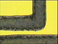
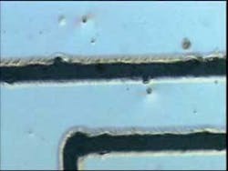
Processing of ITO thin film is demonstrated in Figure 6 where a 20µm groove was processed in a 20nm thick ITO layer with 0.55W@2MHz. The processing was done without any damage to the polymer underneath.
Processing of SnO thin film is demonstrated in Figure 7 where two 12µm grooves were processed in a 600nm thick SnO layer with 2W@2MHz. The processing was done without any damage to the polymer underneath.
In Figure 8 the processing of Ni thin film is demonstrated, with two 30µm grooves processed in 20nm thick Ni layer with 0.8W@2MHz. The processing was done without any damage to the polymer underneath.
Two 30µm grooves were processed to 100nm thick Al layer with 3W@2MHz as shown in Figure 9. Again the processing was done without any damage to the polymer underneath.
Conclusions
Micromanufacturing processes are the fastest growing applications for lasers due to the dynamic consumer electronics market. Thin film patterning is one of the typical examples in these applications. The picosecond fiber laser operating with MHz repetition rate is very suitable for processing thin films. High processing quality combined with industrial grade high processing speeds makes the laser an attractive industrial tool.
Jari Sillanpää ([email protected]) and Harry Asonen ([email protected]) are with Corelase, Tampere, Finland.


