Laser micromachining of thin metals
Fiber lasers show promise as an alternative for metal processing
Several lasers are available for cutting, drilling, welding, and altering the surface of relatively thick metals for use in diverse industries, including automotive, shipbuilding, and medical. However, many emerging applications require very thin metals to be laser-processed with extremely high accuracy and clean edges. In recent years several new laser technologies for laser micromachining have been introduced. These lasers possess excellent mode quality and high focusability-two important capabilities for achieving small feature size and clean edges.
In this study, we compare results obtained using several different kinds of low-power lasers with wavelengths including 355 nm, 532 nm, 1064 nm, and 1.085 micrometer. We focus on cutting complex shapes into various metals of different thicknesses.
The benefits of lasers
Although various techniques are available for processing metals, they all have some drawbacks, especially as compared to lasers. For instance, you can process metals efficiently using EDM (Electrode Discharge Machining) techniques, but this process has limitations in terms of minimum achievable feature size on target. Furthermore, smaller electrodes cost more and break more often than lasers, which adds expense as replacements are required more frequently.
null
Etch techniques also are used to process metals, and these techniques can be cost-effective in some cases, but this process also suffers from some major shortcomings. First, etch processes require multiple steps, whereas laser processing can be accomplished in just one step. Second, one has to deal with both the caustic chemicals and the toxic waste that are generated as a result of etch techniques. Finally, aspect ratio is limited to near 1:1, and even in this case significant undercutting and sidewall taper can exist. Meanwhile, mechanical drilling or routing is limited to about 250-micron diameter features; even though 100-micron drills are available commercially, these bits are expensive and have a short lifetime.
Using lasers to cut metals into complex shapes and patterns affords many benefits. With lasers, drill breakage and tool wear are eliminated. Also, with lasers there is a much lower limit in terms of minimum achievable hole diameter and feature size. Laser drilling also allows you to drill on angled or curved surfaces as well as on hard and soft materials. Plus, the programmable nature of the laser tool allows for very high-speed drilling and routing applications where many thousands of holes are required in short cycle times.
In this study, we evaluated a number of hard-to-machine thin metals, including copper (Cu), beryllium copper (BeCu), phosphor/bronze (Pbronze), molybdenum (Mo), stainless steel (SS), nickel (Ni), aluminum (Al), titanium (Ti), tempered steel (TS), and thin metallic coatings (on hard and soft substrates) of indium/tin/oxide (ITO) and other thin metals. All of these metals are used in both mainstream and exotic applications requiring clean edges and small feature sizes. Very thin films are of great interest. As circuitry gets smaller and denser, material thickness for both dielectrics and conductors also gets thinner. One of the most interesting applications involves patterning of very thin (usually a few hundred Angstroms), conductive materials such as Cu, Au, Ag, and ITO. These metals exhibit interesting properties in thin film form, and they react slightly differently to laser irradiation in thin film form than they do in bulk form. For instance, the energy density required to ablate “thick” metals (more than about 1 micron in thickness) is on the order of several to even tens of J/cm2, while that same metal in thin film form can be removed with fractions of a J/cm2 when applied to a substrate. These thin films are used in products such as touch screens, flat panel displays, aircraft cockpits, and medical devices, to name a few, and more applications are being investigated.
In every case, we used low-power lasers (less than 100 W and, in most cases, much less). Therefore, we restricted the thickness of the metals to less than 20 mils (500 microns). For this study we used the Coherent (Santa Clara, CA) Avia 355nm, 3W laser; the Photonics Industries (Bohemia, NY) 532nm, 7W laser; and the Spectra Physics (Mountain View, CA) 1064nm, 3W laser. We did not use the CO2 laser or the excimer laser for this study. The CO2 laser was reflective with many of the metals we investigated, and the excimer laser is simply too slow to be of commercial value for this type of work.
We also conducted some tests on the 1.085-micrometer-wavelength, 100W fiber laser and we discuss these results as well. Diode-pumped, solid-state lasers, which have good beam quality at short wavelengths, can be focused to spot sizes of 20 microns or less. Because this is much smaller than the features we examined in these tests, we did trepanning or routing in multiple passes. We downloaded DXF files into the PhotoMachining software and added laser parameters. The result is a machine file with all the processing information stored so that these files can be accessed for future reference and use. It is important to note that for all the accompanying figures (with the one noted exception), high-resolution photos were taken with a stereoscope at about 40X magnification directly after laser processing with no post lasercleaning. Therefore, all figures presented should be considered “worst-case” scenarios. In addition, all the figures were made using galvanometer beam delivery and no gas assist.
Laser processing results
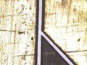
Here we present some results of laser processing, with two different lasers for comparison: the 355nm laser (all the “a” figures) and the 532nm laser (all the “b” figures). Figure 1 shows a representative cut in 125-micron-thick Cu using both lasers; cut kerf is about 75 to 85 microns in all cases. The 532nm laser couples very well and gives faster processing times and cleaner results than the 355nm laser, although both results are favorable. The 355nm laser is favored in printed circuit board applications because the coupling of 532nm light to most dielectrics is not nearly as good as it is using the 355nm UV light.
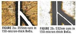
Figure 2 shows the same two lasers used on 150-micron-thick BeCu. Note that the results compare favorably to the Cu results (as do the results with Pbronze, which are not shown). All these Cu metals and derivatives couple well with both lasers, but as a note, we were unable to get any clean processing of Cu metals using the 1.085-micrometer fiber laser, as the reflectivity at this wavelength is much too high.
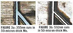
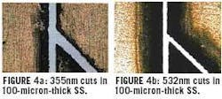
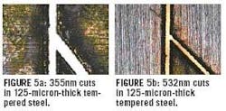
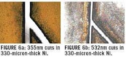
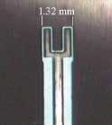
Figure 3 shows the same pattern laser-etched into Mo. The coupling of the 532nm light is not as good as the Cu results noted earlier, although this laser certainly can be used. The results compare to those found for 100-micron-thick SS (see Figure 4) and tempered steel (see Figure 5) and Ni (see Figure 6). Note that Al did not respond well to the 532nm wavelength, while the 355nm laser made very nice cuts in 300-micron-thick material (see Figure 7). For the sake of comparison, Figure 8 shows the same cut as in Figure 6a, using a 355nm laser on Ni, but we used a light acid ultrasound to post-laser-process the material, resulting in a very clean final product. Figure 9 shows a feature in 125-micron-thick Mo that was made using the 355nm laser. Note that the “arm” extends approximately 25mm below what is shown in the picture. This cut was made with so little heat that we saw no lifting effect, as we would with more “thermal” lasers.
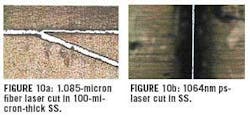
We also looked at results using a 1.5-micrometer fiber laser. In no case involving Cu-based metals could we obtain etching. Nevertheless, in other materials such as SS, tempered steel, and Ni, we obtained excellent results with high (in comparison) processing speeds and good edge quality. We note that in this case, the lab setup was basic and we used a fixed-beam delivery system with high gas assist. We also looked at using a 13ps, 1064nm laser. Cut quality was very good, and although we did not extend the tests to other metals, we believe this laser would be useful over a wide range of materials. Figure 10a shows a cut made with the fiber laser in SS, while Figure 10b shows a 25-micron cut made in SS with the picosecond laser. Note that the results of the fiber laser are not as uniform as the others, but this is an artifact of the quick setup used and should not be seen as a limitation of the laser source.
Finally, Figure 11 shows a complex pattern etched into Au sputtered on Mylar. We can cleanly and easily remove these thin films in very complex and dense patterns using either the 355nm laser or the 532nm laser, depending on the substrate and feature sizes required. Galvanometer-based beam delivery allows easy file transfer and accuracies on the order of 10 to 20 microns (fixed-beam delivery can give accuracies on the order of microns, but at a slower processing rate).
Conclusions
Our conclusions are summarized as follows:
355nm Q-switched lasers gave very good processing results on all metals tested, with small feature sizes (a 25-micron spot). Any metal less than 125 microns thick will process quickly and cleanly. Metals between 5 and 10 mils (250 microns) thick will show clean processing results, but may be somewhat slow for bulk processing. Metals up to 20 mils (500 microns) thick may be candidates for some processing applications, but at reduced speed. And any metal more than 20 mils thick is probably not a good candidate for the Q-switched laser. We do not expect this conclusion to change significantly by using higher-power lasers that are now available, such as 10W or 15W.
532nm lasers also can be used and give very good results on many metals, especially Cu-containing metals. Because of the longer wavelength, minimum achievable spot size for a given optical setup is larger than with the 355nm laser. These lasers are available up to about 15 W with low M2 values (larger lasers are available, but M2 goes up) and can be somewhat cheaper to own and operate than 355nm lasers.
532nm and 355nm lasers are excellent at removing thin films from a variety of substrates. You can use 532nm lasers to shoot through transparent substrates such as glass. 355nm lasers can remove top-side coatings with little or no damage to the substrate, even if the substrate absorbs the UV wavelength.
Picosecond lasers are interesting and provide very clean processing results, but the high cost of currently available sources precludes them from use in all but the most exotic applications.
In short, fiber lasers look like an interesting alternative for metal processing, and these lasers can cut cleanly and quickly, even for metal thicknesses of up to several millimeters. The fundamental frequency cannot be used on metals containing Cu, but future developments in frequency doubling and tripling may make these lasers extremely useful for all metals.
All authors are involved in laser applications at PhotoMachining Inc. in Pelham, New Hampshire. They would like to acknowledge Chuck Ratermann for providing the picosecond-laser photo, and especially William Shiner and Vijay Kancharla for allowing them time in the IPG Photonics applications laboratory for fiber laser investigation.
