Miniaturizing microelectronics
Microelectronics manufacturers are able to advance technology using photonics
Arnd Krueger and Wolfgang Juchmann
Portability is the industry standard in the computer and consumer electronics industry today as laptops, PDAs, and MP3 players have become ubiquitous. Technology in the microelectronics industry is evolving at an exponential pace with ever-increasing demands toward miniaturization, increased storage capacity, faster processing, improved visualization of digital data, and increased communication capability.
Many of these advancements are the result of increased throughput in manufacturing and more efficient use of disk and chip space. Yet, this would not have been possible if not for the breakthrough developments that have enabled microelectronics manufacturers to replace many electrical, mechanical, and chemical processes with superior optical technologies. Consider a typical laptop (see Figure 1). The manufacture of virtually every component currently has been enhanced with at least one laser application, which has changed the way these components are produced.
The two main criteria for microelectronics design are to make components faster and smaller. For the lasers used in the manufacturing processes, this means increased pulse repetition rates for higher manufacturing throughput and smaller spot-sizes (that is, shorter wavelengths) for decreased feature sizes. Developments in solid-state lasers have addressed these demands making a significant impact on the microelectronics industry in applications such as metrology, memory repair, circuit trimming, via-hole drilling, hard disk texturing, and subcomponent marking. The production of flat panel displays (FPD) alone involves several laser applications, including laser annealing, glass separation, and marking. Q-switched diode-pumped solid-state (DPSS) lasers have become the industry standard in many of these applications, as repetition rates have increased and reliable solid-state UV sources are more readily available.
Now more than ever, the promise of photonics in industrial applications is being realized as the laser’s role expands from a research tool and heavy-duty machining device to an enabling technology in a broad range of micro-industrial processes. Companies such as Newport (www.newport.com) and its Spectra-Physics Lasers Division (www.spectra-physics.com) have been developing lasers and photonics components for more than 40 years, and are now playing an even larger role in the microelectronics industry, as they are able to combine robust solid-state laser sources with vibration control, opto-mechanical, and laser positioning equipment into OEM subassemblies for system integrators and capital equipment suppliers.
DPSS lasers in manufacturing
Replacing chemical and mechanical manufacturing processes with laser-based solutions yields several advantages over traditional technologies. DPSS lasers have become a powerful manufacturing tool because of their compact size, robustness, beam quality, and flexibility of repetition rate and wavelengths. Today, UV wavelengths (mainly 355 and 266 nm), have become more important in microelectronics manufacturing because they enable smaller spot sizes.
Laser micromachining is a non-contact process: no water is needed, little to no particle dust is produced, and hazardous chemicals become unnecessary. Laser-based manufacturing steps are “cleaner,” as they frequently replace wet chemical procedures, but they also enable better process control. Laser scribing, texturing, and marking allow for smaller and more precise features in a more regular arrangement using significantly less space on the individual device. This results in improved quality control, higher yields, and increased throughput. In addition, there are some laser-based manufacturing applications that cannot be accomplished in any other way, for example high-resolution photolithography.
Laptop computer
To illustrate the importance of photonic applications in microelectronics manufacturing, we will use the example of a typical laptop computer, and outline some of the manufacturing steps that today rely on laser processing, including the production of the hard drive, dynamic random access memory (DRAM), keyboard, PCB, and flat panel display.
In the manufacturing of a laptop many individual pieces are produced, and laser marking of these components provides a date and time stamp or other alphanumeric symbols. This dye-free process is routinely used in marking of electronic component packages and keyboards. Similarly, semiconductor wafers are marked with a green (532 nm) Q-switched laser. Here, the light source is used on the back side of a wafer to avoid potential damage to the active side, and unique identification is added to each chip on the wafer.
Marking, or “titling,” is also used to trace FPDs. In this application, manufacturers require solutions that minimize the amount of surface area affected on the FPD. As a result, many companies use UV lasers, which deliver the smallest spot size available today. A number of different laser titling techniques are currently used by the FPD industry. In some cases the glass is coated with a UV-sensitive material, while other manufacturers laser etch the glass directly, either on or below the glass surface.
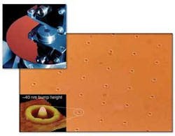
Hard disk texturing is a process that produces a texturized or “roughed-up” zone, which functions as a landing zone on the hard drive (see Figure 2). Without this technique, the highly polished surface would lead to adhesion of the read-write head to the hard drive. During boot-up of the computer, when the hard disk starts spinning, the read-write head could damage an untextured device. In the past, hard drive manufacturers had to rely on diamond slurry for grinding of the surface. For some years, however, texturing with lasers has replaced this wet process.
Laser disk texturing requires high pulse repetition rates for increased processing throughput, high reliability to reduce manufacturing down-time, and high pulse-to-pulse stability and precise control of the pulse duration to ensure reproducible feature formation. High repetition rate also means the ability to produce higher density landing zones, as more features can be produced in the same time. Currently texturing in the hard drive industry is accomplished with Q-switched DPSS lasers such as the V-series made by Spectra Physics that is able to produce an average power of up to 8W at 1064 nm with excellent pulse-to-pulse stability at repetition rates as high as 300 kHz. The laser beam is close to diffraction-limited (TEM00), enabling the reproducible formation of round “bumps.” This laser is currently the industry standard with more than 90 percent of the total market share in the hard disk manufacturing industry.
PC board manufacturing
Many steps in the manufacturing of PC boards use laser processes, including integrated circuit marking, memory repair, silicon wafer dicing, and resistor trimming.
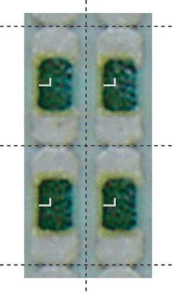
Components on PC boards are shrinking, and in many cases the exact resistive and capacitive values of components can not be obtained in a direct manufacturing process. Instead, resistivity is optimized by a two-step process involving on-line measurement and trimming. Manufacturers of small precision resistors and capacitors establish the exact values by selectively removing bulk material (laser trimming), in an “L” shape (see Figure 3), using an IR Q-switched DPSS laser such as the Navigator Series by Spectra Physics. Laser trimming demands a consistent pulse width and excellent beam quality for efficient and reproducible processing.
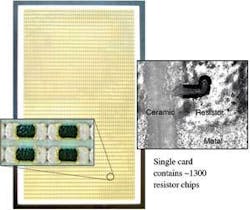
After the components are optimized, a laser is used to perforate or scribe the ceramic substrate to separate the individual chips. The scribe is a partial cut or perforation. Later in the process mechanical pressure is used to separate the individual components (see Figure 4).
Similarly, semiconductor wafers are scribed and diced using lasers. Laser wafer dicing offers several advantages over the diamond saw alternative. With the traditional method the blades become dull and need replacing-sometimes after just one or two wafers. This means extra manufacturing costs due to blade replacement and substantial downtime. Laser dicing is a non-contact method without consumables. Non-contact methods produce little or no dust, and result in cleaner edges; improved edge quality means less damage and better yield. In addition, thin semiconductor wafers can not be cut using a traditional mechanical saw, and a UV or IR laser is essential to separate individual chips on a semiconductor wafer.
Memory repair
In the production of memory chips, there are sectors of the chip that are damaged or redundant. A laser beam is used to blow out specific circuits or fuses, thus isolating or disabling damaged memory sectors, resulting in significantly higher yields. Traditionally memory repair was accomplished using an IR laser, but advances in reliable solid-state green (532 nm) and UV (355 nm) sources have provided the smaller spot sizes needed to selectively destruct smaller fuses in smaller and more densely packed memory sectors-thus enabling further miniaturization in the microelectronics industry. Current industrial processes demand single pulse processing, thus requiring a laser with excellent pulse-to-pulse stability and a well-defined round beam.
The next step
As microelectronics processing evolves, more manufacturing processes that currently use IR or visible wavelengths will change protocols and materials to take advantage of the smaller spot size of UV wavelengths. Increasing repetition rate is one path for higher throughput, yet other possibilities also exist. By changing industrial processes to utilize a single high-power laser as a one-source “light engine” for multiple workstations, a further increase in throughput is achievable.
Lasers continue to evolve, delivering higher power in smaller packages, and enabling even broader adoption of photonics technologies into industry applications. As laser technology develops it will no doubt enable further advances in microelectronics hereto unforeseen.
The number of applications that laser and laser systems companies serve will continue to increase as smaller, faster, more powerful, more flexible, and more reliable light sources are developed. Continued development of subsystems, which include optics, motion control systems, and vibration isolation solutions will provide complete “light engine” subsystems, which will be utilized by systems integrators and capital equipment manufacturers to further advance their own technologies and applications.
Arnd Krueger ([email protected]) is senior director of product marketing and Wolfgang Juchmann is product manager for solid-state lasers at Spectra Physics.


