The expanding role of excimer lasers
Unlike most other gas lasers, the number and diversity of excimer laser applications continues to grow. This is because excimer lasers offer unique characteristics and capabilities that make them applicable across a wide range of materials processing needs and provide unique capabilities that make them well suited to emerging technologies. There are two main areas of interest, 1) materials removal and 2) photonic materials alterations especially drilling, scribing, micromachining, and other operations where feature sizes have become miniaturized beyond the range of mechanical tooling. The nature of excimer material removal—photo-ablation, with little or no heat-affected zone—plus the clean, precisely defined cuts characteristic of excimers, make them ideal for micromachining sub-micron resolution features. Moreover, short-wavelength ultraviolet (UV) excimer radiation is readily absorbed by many materials, resulting in efficient processing: from hard materials such as silicon and ceramic to soft polymers. The wide range of available UV excimer wavelengths means that an appropriate wavelength can be chosen for virtually any material processed. And the nature of the large, multimode, top hat excimer beam allows shaping and masking techniques for large-area patterning for efficient manufacturing, micromachining of complex, 3D features.
Currently, there are three major applications for excimer lasers: LASIK eye surgery, flat panel display annealing, and semiconductor microlithography. The remainder of the excimer market, which is nevertheless quite substantial, consists of a diverse set of processes and industries, ranging from marking eyeglasses to treating diesel cylinder liners, to via drilling in the electronics industry. While the “big three” applications are serviced with dedicated models optimized for a well-established set of performance parameters, the vast majority of applications have a wide and diverse range of laser requirements. That’s because for a given material and wavelength, effective materials processing requires the right balance between key excimer laser characteristics, pulse energy (fluence on target), and repetition rate.
Energy or repetition rate?
Initially, industrial excimer lasers were mostly characterized by either high pulse energies (hundreds of millijoules) at modest (hundreds of Hz) repetition rates, or high repetition rates (100 Hz–2 kHz) and pulse energies of a few millijoules. But the maturation of LTPS (low-temperature polysilicon) annealing for flat panel displays drove the development of lasers that offer both high repetition rates (up to 300 Hz) and high pulse energies (>1 joule). These are now being employed in micromachining applications such as direct patterning of thin films, primarily in electronics.
Another important trend has been the development and steady improvement in cost-effective “mini-excimers” that offer pulse energies around 10 mJ, maximum repetition rates of a few hundred Hz or more, a beam height of only 9-10 mm, and a small overall package. Today, these lasers are now particularly economical to operate because of key improvements in long electrode (tube) lifetimes, overall efficiency, and long gas-fill intervals. Plus these lasers use a smaller volume of gas and can use smaller-diameter beam delivery optics.
Unique characteristics
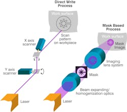
The rectangular output beam of an excimer laser can extend to several centimeters in its largest dimension. This factor, combined with an excimer’s high pulse energy and lower repetition rates, enables excimers to be optimally used with photomasks for producing highly repetitive patterns over an extended area (see Figure 1). Conversely, the beam produced by many solid-state lasers is usually focused to a small spot and scanned with galvo mirrors. This is called direct writing (see Figure 2), and the pin-point nature of direct writing has its own specific range of applications, such as wafer scribing and dice singulation. However, direct-write micromachining has the disadvantage of not being able to remove larger areas with smooth depth control as the rastering of the small beams leave grooves.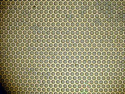
3D-patterning can be achieved with the convolution of the image masks to generate smooth surface complex features. For instance a triangle convoluted along its apex will generate a ‘V’ groove. A square will generate a flat-bottom groove, and a circle will generate a groove with a parabolic bottom geometry.
Choosing the wavelength
Excimers offer wavelength outputs from 157nm to 351nm. Choosing the optimum wavelength for a specific task often involves a trade-off between the quality of results achieved (that is, less peripheral thermal effects and sharper, cleaner edges), overall efficiency, and process cost. For example the optimum wavelength will often improve not only the overall quality but also the process speed by allowing lower energy to do the same amount of work.
In UV laser micromachining applications of thermally sensitive materials or highly transparent materials, the general rule is that shorter wavelengths produce a better result. This is why 193 nm is preferred over longer wavelengths for marking and drilling glass and sensitive polymers such as PET, PMMA, and these types of plastics and 157nm is preferred for Teflon, polyethylene, and quartz,
However, the specific characteristics of certain materials cause them to favor specific wavelengths; absorption is key. For example, Teflon, which is used to coat medical implants and as an insulator in RF devices, has a low absorption of visible or most longer ultraviolet wavelengths. For this material, 157nm is the preferred wavelength. For many plastics, matching the laser line to a maximum in the absorption spectrum can result in better results and faster throughput. An example is PMMA, which has an absorption maximum at 222 nm, making the oft-forgotten KrCl line at 222 nm a great choice for this material.
With excimer lasers, longer wavelength usually means lower operating costs, in terms of laser tube life, gas lifetime, and beam delivery optics. And it is useful to remember that using chlorides will result in greater laser longevity and lower operating costs compared to fluorides.
Applications diversity
Manufacturing applications for excimers are mainly in the areas of micromachining (including marking) and material/surface transformation. Excimer micromachining can create holes, grooves, and other 3D complex features with sub-micron depth precision when used in conjunction with active feedback (for example, laser metrology) to control dosing.
The use of short wavelengths enables sub-micron lateral resolution; however, sub-micron performance depends on more than just the laser. It also requires high-fidelity motion control, usually with air-bearing stages to move the substrate, and lenses that combine the requisite depth of focus with a sufficient field of view for practical throughput.
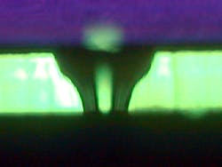
Excimers are especially well-suited to applications involving large-areas and dense, repetitive patterns. One example is via drilling in multi-chip modules. This application has been dominated by systems using solid-state or CO2 together with galvanometer scanning. However, electronic device features (including vias) are shrinking while production volumes are increasing. The increased volume of high-density parts with smaller vias is an example where excimer patterning becomes very competitive over other direct write techniques. For example, with use of a photomask in conjunction with “step and repeat” substrate motion, excimers can generate >10,000 vias per second. This massive parallel drilling capacity (see Figure 1) is also employed to create filters that serve as particle traps in inkjet printers and for a new generation of medical inhalers currently undergoing FDA review.
Miniaturized cell culture tools, often referred to as ‘lab on a chip,’ are fabricated in polycarbonate and other plastics with 248nm excimers. Here, a single laser may be used to create wells and microchannels, as well as micron-sized through holes (see Figure 4). These through-holes are then blocked with metal deposition techniques to provide both a hermetic seal and electrical conduction path.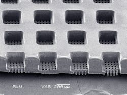
Another rapidly growing application is direct patterning of thin films, whereby laser energy penetrates the thin film and is absorbed at the interface by the underlying material. The sudden vaporization of material at the interface results in removal of the film. This excimer “TFA” Thin Film Ablation process works best for films that are thin-typically less than one micron. In these cases the energy required to remove/pattern the film is less than that required to vaporize the equivalent volume of the same material. Examples include metal films (up to 1000 nm thickness) on dielectric substrates for applications such as RFID circuits and medical sensors. Where necessary, the thickness of the metal is then augmented through a low-cost plating process. Other combinations include patterning dielectrics on metals, polymers on ceramics, and even polymers on polymers. Most of these applications are performed using a reel-to-reel material handling process wherein each film location is processed in a single laser pulse.
Excimers are also unique in their ability to transform surface and sub-surface materials; one example is case hardening high-carbon steel parts. Un-annealed, these steels contain large crystals of iron and carbon. A 308nm excimer laser can bring the surface layer of the metal above the eutectic zone at the microscopic level, leaving atoms free to migrate within the metal. For carbon steel the process involves only carbon and iron. Here the case hardening delivers a homogenous matrix that remains at the surface while the core materials retain the malleability of unhardened steel.
For other high-harden-ability metal alloys, materials such as chromium (or other metals) can move to the surface creating a unique surface that may be harder, more chemical resistant, or more lubricious, for instance. At the same time, the bulk of the part is unaffected and maintains the desirable malleability that is characteristic of these steels. 308nm excimers are also used to create low-friction surfaces on cast iron diesel engine cylinder liners. This Audi-developed application was described in some detail in Industrial Laser Solutions magazine (October, 2004).
Another surface modification application is micromachining or planarizing CVD diamond wafers, whose poly-crystalline nature results in an initially rough surface. 193 nm is preferred for the highest-purity diamonds. 3D micromachining of wear surfaces, wire dies, heat sinks, and cutting tools are some examples of high-precision micromachining. In the case of linearization, a 193- or 248nm excimer laser beam is conditioned into a line and is positioned to impact the overall surface at or below the critical angle. Simple optics theory dictates that a smooth surface will therefore be totally reflective, whereas rough spots will enable the laser to be absorbed by the material. The result is a smooth surface and completely self-terminating process.
The diverse nature of industrial processing tasks using excimer lasers drives the demand for products with a wide range of output characteristics. Virtually all these applications share a common need for high reliability, longer laser life, and lower operating costs. Driven by three dominant applications, laser manufacturers have responded with a number of significant technical enhancements. The result is a new generation of excimer lasers offering extended maintenance intervals, more advanced self-regulation, and lower cost of ownership.
About the Author
Matthew Philpott
Chief Marketing and Sales Officer, NUBURU
Dr. Matthew Philpott is chief marketing and sales officer at NUBURU (Centennial, CO). He has 22 years’ experience in the laser industry, most recently focusing on the electric vehicle market for Coherent. He led a multi-year global team effort to grow Coherent’s business, making it one of the top suppliers of lasers for battery manufacturing. Beyond success in the EV market, he has held a wide range of roles in sales, marketing, and business development, with expertise in materials processing, microelectronics, display, and bioinstrumentation. Dr. Philpott holds a B.S. in chemistry and a Ph.D. from the University of Washington in physical chemistry.
Jeff Sercel
President, IPG Microsystems LLC
Jeff Sercel is president at IPG Microsystems LLC (Manchester, NH); he previously served as chairman and CTO of J. P. Sercel Associates (JPSA; also in Manchester, NH).
Ruediger Hack
Vice President Sales and Marketing, Bruker Nano Analytics
Dr. Ruediger Hack is vice president of sales and marketing at Bruker Nano Analytics (Berlin, Germany area). From 2004 through 2008, he served as worldwide director of sales at Coherent (Munich, Germany area).