New Tool for the Toolbox
Picosecond lasers for micromachining enable reliable production built on the fast and basically non-thermal removal of many industrially relevant materials
Bernhard Klimt
Ultrashort-pulse lasers have been commercially available since the early 1990s. Their pulses cause a light-material interaction faster than characteristic thermal processes.1 This produces minimal thermal impact and outstanding micromachining quality without burr, recast, and thermally induced micro-cracks.
Nd:Vanadate lasers with 10ps pulses can micromachine most materials with quality results,2 and their higher output powers, with very good beam quality, at repetition rates of several 100kHz are meeting the requirements of industrial micromachining.
The most important laser parameters for industrial micromachining applications are pulse energy, spot size, laser wavelength, and pulse on demand operation. The basic event is ablation of a thin material layer in the focus spot. High process quality is achieved by ablation close to threshold,3 where the ablation depth per laser pulse is on the order of tens of nanometers, thus offering a high-resolution process. Any 3D-micromilling of material is accomplished by overlapping this basic event appropriately and repeating it with the high pulse rate of industrial picosecond lasers.
This basic ablation event has a threshold in the order of 1J/cm² (for 10ps pulse), between about 0.2J/cm² for metals, and several J/cm² for glasses and ceramics. Energy density is controlled by pulse energy and spot size. The pulse energy has to correspond to the spot size and match the 1J/cm² threshold criterion; 10µm diameters for micromachining need about 1µJ.
Gentle ablation, close to threshold, needs high repetition rates to achieve high average power and throughput. Even at constant average power, experiments indicate that combining higher pulse rates at smaller pulse energies achieves quality at higher ablation rates. Lasers with a pulse burst mode are more valuable for ablation.4
Generation of shorter wavelengths results in about 50 percent pulse energy conversion but better focusability. Typically, metals can be well machined with 1064nm radiation; other materials may need operation at 532 or 355nm.
The throughput of a micromachining application is a function of ablation rate and power applied. As a rule of thumb, an 8W picosecond laser can remove about 1mm³ of material (steel) per min. For other materials it is similar, as long as the structures are shallow; structuring clean edges often reaches only about 0.1mm³/min.
The total cost of ownership for such an 8W picosecond laser can be about 15$/h. Therefore, all applications that generate enough added value by the precise ablation-removal to justify the relation 1mm³-1min-0.25$ (with one 8W picosecond laser) benefit potentially well from picosecond laser micromachining.
Application examples
Picosecond lasers can be used to drill, cut, and structure thin layers of special materials to create highly defined apertures, electrodes, contact layers, and such. They are employed in the manufacture of masks and test plates for the semiconductor industry. They cut medical stents and drill inkjet nozzles5 or fuel injection nozzles. They are used to produce filters with identical openings. They treat carbide tips and other hard metal tools to improve their quality and multiply their useful life.6 Picosecond pulses can be used to structure the surface of machine parts for friction reduction, or machine diffraction gratings.7 They can produce identification marks and structure thin layers used in semiconductor, solar cell, or display technology.8
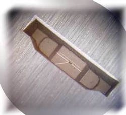
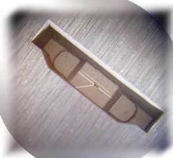
Metal machining - Stainless steel, aluminium, copper, brass, molybdenum, titanium, tungsten, and various alloys have been cut, drilled, milled, or structured with high accuracy and minimal thermal impact using picosecond lasers. The ablation threshold for these metals is in the range of 0.2-0.5J/cm². In Figure 1 a micromold is machined with 1W@500kHz, 1064nm, in a 20µm-spot. After material removal of about 2mm length x 700µm width x 600µm depth, an ablation rate of about 0.1mm³/min was calculated.
Figure 2 shows the drilling of a 170µm diameter hole into 100µm molybdenum foil with 0.55W@ 355nm; processing time was 8 seconds.
Circular geometry, sharp edges, small taper, and no burr or recast can be observed in the SEM picture. Accurate material removal also allows to machine blind holes, countersinks, or user-defined trailing edges. Drilling holes with higher aspect ratios requires trepanning optics.
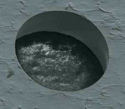
Polyimide machining - Cutting Kapton foils with acceptable quality is achieved with UV laser, but 3D machining of Kapton requires a non-thermal ablation process. With picosecond lasers (see Figure 3) no molten material, burr, or recast is visible. 300mW@100kHz at 355nm was used to machine these blind holes in Kapton.
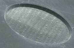
Glass machining - Precise glass microstructures used in biomedicine, biochemistry, sensors, and MEMS devices can be machined. Figure 4 shows a microtrench machined into borosilicate glass with a picosecond laser (355nm, 100mW, ~15µm spot size).
Picosecond laser pulses from the Lumera RAPID also have been used to melt glass, create waveguides, and microweld glass.9 Crack-free microwelding with speeds of up to 100mm/s was achieved with 0.7W@1064nm.
Silicon machining - In the future very thin wafers (40µm), used in semiconductor and solar cell technology, will have to be cut with small kerfs and high edge quality. The picosecond lasers will be able to machine such wafers without microcracks.
New industrial processes and devices
The option to locally and gently remove or modify very small layers on/in materials with a software-controlled laser beam enables new industrial processes and devices. A large-scale industrial application potential is in solar technology. Engineers in the photovoltaic industry are trying to improve the cost-efficiency ratio by combining advanced back-contact solar cell designs (see Figure 5) with large-scale production techniques and the use of cost-effective Czochralski silicon material.10
Such design goals require a layout with relaxed carrier lifetime specifications. That can be achieved by using thin cells with tight rear side patterns. Non-contact, gentle removal of prices structures on ~100nm thin layers of silicon oxide or silicon nitride with high throughput and fine quality (minimum effects to the remaining structure) is needed. The use of high-power picosecond lasers with high PRF is a promising approach.
Modern large inkjet printer heads require prolonged life of the individual inkjet nozzles. Therefore, they are machined in steel foil by picosecond lasers, not in polyimide by excimer lasers as has been the case.5
Conclusion
Picosecond lasers belong in the toolbox of manufacturing engineers. They enable reliable production built on the fast and basically non-thermal removal (or modification) of many industrially relevant materials.
As new ultrashort-pulse lasers with higher power and higher repetition rate will enter the market, reliability will be further improved. A diversification of models to match different applications can be expected. Based on these sources application engineers will develop new industrially relevant processes and scientific and manufacturing devices.
References
- Breitling, D., Ruf, A., Dausinger, F. (2004) “Fundamental aspects in machining of metals with short and ultra short laser pulses,” Proc. of SPIE Vol. 5339, 49-63.
- Knappe, R., Herrmann, T., Henrich, B., Nebel, A. (2005) “Novel picosecond lasers for fast micro-machining,” Proc. of Third International WLT-Conference On Lasers in Manufacturing.
- Gu, B. (2005) “Ultra fast laser processing for next generation memory repair and semiconductor manufacturing,” Proc. of SPIE Vol. 5714-04.
- Herrmann, T., Haloui, H., Knappe, R., Henrich, B., Nebel, A., “Improved picosecond laser radiation for micromachining,” M1003, ICALEO 2006.
- Liu, X., “Industrial applications of ultrahigh precision short pulse laser processing,” Panasonic, Photonics West 2005.
- Tönshoff, H. K., Ostendorf, A., Kulik, C., Siegel, F. (2003) “Finishing of cutting tools using selective material ablation,” Proc. of the 1. international CIRP seminar on micro and nano technologies, 77-80.
- Noh, J., Sohn, H., Suh, J., Lee,. J.-H. (2006) “Application of picosecond laser micro-machining for diffraction gratings,” The 4th International Congress on Laser Advanced Materials Processing, Kyoto, Japan, p. 262
- Raciukaitis, G., Brikas, M., Gedvilas, M., Dracianovas, G.; “Patterning of ITO layers on glass with high repetition rate picosecond lasers,” LAMP 2006, Kyoto.
- Miyamoto, I., Horn, A., Gottmann, J.; “Local melting of glass material and its application to direct fusion welding by ps-laser pulses,” LAMP 2006, Kyoto.
- Huljic´, D. M. et al., “Development of a 21% back-contact monocrystalline silicon solar cell for large scale production,” 21st EU-PVSEC, Dresden 04.-08.September 2006.
Bernhard Klimt is with Lumera Laser GmbH, Kaiserslautern, Germany. Contact [email protected].
