Lasers in failure analysis
by Greg Anderson
By bringing vision, lasers, and laser pulse shaping technology together with software and hardware for mold compound removal, failure analysis is reaching new levels of reliability, speed, and ability
Most industries have what could be termed “necessary evils”; those activities or costs that produce no return on investment, in the strictest sense of the word, but are indispensable in the life of a company. The semiconductor industry has one in its Failure Analysis Laboratory, where prototype designs, current production ICs, and other electronic devices are analyzed to determine why they failed so that an immediate fix can be implemented in current manufacturing or design engineering. Should the failure be caused by the user, warnings are issued to customers on the proper use and specifications for a given product.
Any technology that can enhance, expedite, update, or reduce cost is a very good thing, especially when equipment required for these tasks can cost in the millions of dollars and time is of the essence. A new patented laser method embodied in Control Systemation's FA Lit laser decapping and cross-sectioning tool is just such a technology.
The core of failure analysis is to be able to provide a method or process that enables an integrated circuit to be viewed physically, probed electrically, and actually run live to test and determine defects. The key to this is the removal of the mold compound used to encapsulate or package the die and other components that comprise the IC design. Mold compound is the dark brown or black epoxy-and-sand-based encapsulate that contains the brains of an IC—the die, wires, bonds, and other components that make up an integrated circuit.
By bringing vision, lasers, and laser pulse shaping technology together with software and hardware aimed at enhancing, replacing, and providing new alternatives to the traditional methods of mold compound removal, failure analysis is reaching new levels of reliability, speed, and ability.
One of the most important things that lasers bring to the table is their wavelength. All materials absorb a certain range of light wavelengths and reflect others. Mold compound absorbs the IR wavelength of the decapping laser and the internal components such as copper or gold wires and bonds reflect that wavelength. Thus this unique process is able to ablate or vaporize the compound without damaging or affecting the gold, copper, and aluminum components encased within.
Acid has been the usual method of removal, until the introduction of laser technology into the failure analysis lab, but its disadvantage is the acid itself. Employees must wear protective gear such as hoods, gloves, or full body suits to perform this task and a room must be provided built to specific codes. The process itself is lengthy and difficult, many times taking up to several hours. There are also EPA issues with disposing of the waste produced. Any reduction in the amount of chemical required to complete a removal task is a big cost savings in all of these areas.
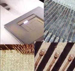
Die bonds and lead bonds are typical area for defects. This is where a small wire (as small as 25 microns) goes from the top of the die to an area on the substrate that connects to a lead that goes to the outside of the IC; these are the prongs that are soldered or attached to a customer's printed circuit board (PCB) (see FIGURE 1). These wires and bonds are internal to the mold compound of the IC.
When acid is used to remove the mold compound over these potential defects it can also damage the area where the wire is bonded to the die or substrate. It is then impossible to determine if the defect was already there or was caused by the acid.
With a laser and its pulse shaping characteristics adjusted correctly there is no damage to the wires or bonds (see FIGURE 2), so any subsequent pull tests or cross-sectioning results are valid. This is especially true if the wires are copper, which is the new trend in IC design due to cost.
Many IC designs involve components that are at different levels, such as stacked dies or multiple dies. When using acid it is difficult or impossible to target a specific area and then repeat the process on another area, therefore components at multiple levels that require exposure must be done at the same time. Because the acid must be applied for the length of time required for the component at the lowest level to become uncovered, significant damage is incurred by the components at higher levels because they are over exposed.
Laser processing has no such problems. The FA Lit can easily address specific areas and depths with no adverse affects (see FIGURE 3).
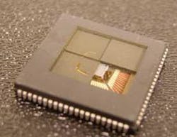
Another situation where acid is a problem is exposing a component that is at one corner of an IC (see FIGURE 4). Acid can leak over the edge of the device and cannot be made to remain in place long enough to complete the removal task.
The laser beam can quickly and efficiently uncover specific areas such as a bond wire or bond pad. If it is a die or some other sensitive component a pocket can be created that will trap and contain the small amount of acid required to finish the process.
Some dies are covered with a special clear, protective, gel-like substance and then encapsulated with mold compound. This gel is impervious to acid, Reactive Ion Etch (RIE), and in its normal state even a laser beam. However by utilizing a “cold plate” option that is available on the FA Lit this gel can be frozen and in this state is easily removed with the laser (see FIGURE 5).
Some dies are extremely sensitive to any heat that might be transmitted through the bond wires; here the “cold plate” can be used to protect them. By cooling the outside leads any heat generated up at the die bond wires is dissipated.
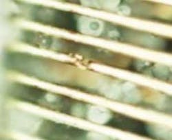
In the design of certain ICs there is a thin layer of “tinning” or silver solder on the bond pad that the outside lead is attached to. This microns-thick layer has a very low heat threshold so the “cold plate” option is used to prevent this layer from melting as the laser removes mold compound around the bond area (see FIGURE 6Integrated circuits where the mold compound is part of the mechanical strength and structure of the IC itself can be very difficult to process using acid, especially when a full decap is required. As soon as a majority of the mold compound is removed the IC literally falls apart. The laser beam offers the ability to remove compound in complex patterns exposing all the pertinent components but leaving a structural band that ties the layout of the IC together. The laser can place this configuration in a location that does not require analysis allowing the IC to be handled for further testing.
A challenge in the Failure Analysis lab arises when there is only one part to analyze. If the process fails, destroys, or alters the device or component, the chance for analysis is lost. Laser compound removal is precise, it targets a specific area and has controls that allow a fast removal at the start and then adjusts to a slow and careful real-time process. The chances of getting it right the first time are exponentially increased over current processes. The swiftness of the process (seconds as opposed to minutes and hours) is a bonus.
These assets also provide the lab with tools that can be utilized in unique and unexpected ways. For example acid or RIE has no chance in one IC where glass covers the die attached to the IC substrate with epoxy allowing light to transmit directly onto the die. The decapping laser's wavelength allows transmission through the glass to break the epoxy bond and the glass cover pops right off.
Another application involves ICs that have a metal lid or cover over the die and the laser beam's ability to be directed at specific areas with specific shapes or patterns. Four small circle shapes are directed over the four adhesive points that attach the metal cover to the substrate. A few seconds beam power brakes the adhesion and the metal lid is easily removed.
Another situation requires the IC being tested to remain 100% intact; this is critical to the failure analysis test procedure. The suspect defect was bond and wire. 137 of the 150 or so wires on this part had a defect and a physical probe performed the test. By importing an X-ray image of the defect and overlaying it on the actual part, the laser beam removed the compound only over that one bond and a probe confirmed the defect. FIGURE 7 shows defect with a full decap.
While failure analysis does not have a direct “Return on Investment” such as a piece of capital equipment, its contributions to streamlining the development of a new design or its speedy determination of a major and costly manufacturing problem enable it to sometimes have a greater impact on “ROI” than many significant capital expenditures.
Lasers have increased output and they perform tasks never before possible. As the laser's capabilities are more steadily used in the failure analysis lab greater enhancements will be achieved and even more unique and beneficial processes will emerge.
Greg Anderson is president of Control Systemation Inc. (www.controlsystemation.com), Orlando, FL.


