Laser structuring interconnection circuits
Lasers offer an alternative method for producing electrical patterns
by Pascal Metayer and Jacquelot-Damien Lagrange
Ceramics, because of their high dimensional stability, are often used in the field of microelectronics as circuit carriers. These carriers are usually manufactured in the same way as integrated circuits (ICs); a metallization layer is deposited on the ceramic carrier, a resin mask is then applied and etched by photolithography according to the required electrical pattern. The unwanted metal areas are then dissolved in chemical solutions leaving the conductor lines. The advantages of this technique are high resolution and batch-processing capability of multiple circuits that leads to unit cost reduction. Disadvantages are it is mainly suited for substrates in plane formats and the process requires large production quantities in order to amortize the cost of photolithography masks.
There is another method for producing electrical patterns—using a laser beam to directly etch the metal layer without using a mask. This process is called laser micromachining or laser ablation, because metal is ablated, and it offers a high flexibility of use and is well suited for fast prototyping. A laser makes it possible to achieve uninterrupted paths over several planes of a three-dimensional carrier. And laser ablation allows the engineer to manufacture 3D packaging for microelectronics components. Solid-state lasers are mostly used for micromachining applications because they feature precision, speed, and selective etching.
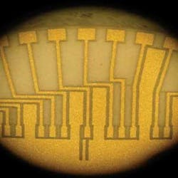
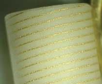
Microcertec currently uses a Nd:YAG laser with 60W output, enabling the etching of thin-film metallized layers with thickness up to 5 µm. When thicker layers are required, additional electroplating is necessary after etching. This laser allows us to make very small features. FIGURE 1 shows straight tracks that are 100 µm-wide with insulation spacing as small as 100 µm. Lateral resolution is a few microns. The interconnection pattern shown here is peripheral on a 30mm-diameter disc on two faces. The ablation process lasts about 20 minutes.
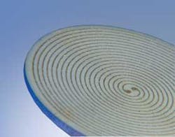
Laser ablation is a technology for structuring tracks directly on the substrate. It allows patterns to be rapidly etched and limitless beam displacements to be programmed. The only required tooling is a jig for holding the part. As a consequence, costs and lead times for set-up and masks are reduced, thus making the process of interest for fast prototyping. The track shown in FIGURE 2 was achieved by programming.
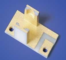
Laser structuring can easily etch areas that cannot be treated by photolithography. As shown in FIGURE 3, laser ablation enables reaching two metallized areas located on different heights by changing the focal plane.
Pattern continuity
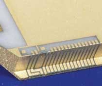
Laser etching is a perfect technique to get pattern continuity over adjacent faces of a monolithic carrier. The most representative example is the achievement of a connection track running along a step. FIGURE 4 shows an array of conductors on the vertical face that enable electrical continuity between two horizontal faces. A continuous track around a cylinder was also made possible with the laser technique, as shown in FIGURE 5.
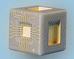
Laser ablation technology helps the engineer to go even further and develop designs that cannot be manufactured with chemical etching technology. As shown in FIGURE 6, ceramic carriers can be made on which conductor lines interconnect several faces of the component thus creating a genuine microelectronics circuit. This a concept that Microcertec calls three-dimensional interconnection circuit or “CI3D”.
Laser etching requires that the engineer has a good knowledge of the metals to be etched as well as the substrate material. Experience makes it possible to etch thin-film layers without damaging the substrate and with little thermal impact on edges of the tracks. It also allows the implementation of efficient cleaning procedures that do not attack the interconnection tracks.
Applications
These products result from combining the technologies of precision grinding of ceramics and laser ablation of metallized thin-film layers. The carrier geometry and interconnection circuit are defined by the customer, thus making it a customized product. Typical applications are found in military, medical, and optoelectronics devices.
A circuit carrier is therefore made available to the final user who can bond onto his microelectronics components—sensor, calculator, chip, LED, and so on—according to his own interconnection pattern. The demand for such products results from either the need to have mechanical and electrical functions together on a same carrier or achieve miniature electronics packaging. The ceramic carrier also offers dimensional stability as well as high electrical insulation. And finally, the etching of distinct and complex interconnection patterns on each of the faces represents programming time only but no additional mask costs.
This concept meets the need to either position microelectronics components in relation to each other in space or offer a simplified solution for the substitution of hybrid components. It is also suited for the manufacturing of components in production quantities of up to a few thousands per month.
Dr. Pascal Métayer and Jacquelot-Damien Lagrange are with Microcertec S.A.S. (www.microcertec.com) located in Collégien, France.

