Laser opportunities in the solar industry
Today solar market reports paint a very different landscape for the industry compared to 2008,1 and the quick conclusion is to link this to macroeconomic meltdown affecting other sectors. But not so fast! Yes, equipment supply has taken a nosedive this year, but mainly because of massive over-capacity from production line suppliers dating back to 20072; when demand was growing faster than production with generous incentives (especially Spain) fueling ambitious expansions. So, by the start of 2009, supply was being forecast to exceed demand by some margin. For established producers, this caused a halt in expansion and prioritizing utilization rates.3 (The turning point had long been predicted as cyclic supply/demand dynamics kicked in.) Because c-Si panels account for 85–90% of cell production4, the impact on tool suppliers here was immediate. But for laser-specific tooling, alarm bells were less audible and cause for optimism has in fact emerged. For thin-film equipment, laser-based tooling was hit quickly, and with low utilization rates across this segment, the consequence for equipment suppliers could be longer term.
Over-capacity coincided with economic downturn late in 2008, causing minor panic within the industry5. Collectively, this double-whammy had greatest impact on producers dependent upon credit for new facilities or technologies; the effect on thin-film equipment showing frightening similarity to consumer electronics6. This has definitely hit those laser-based suppliers historically dependent on thin-film expansions, and has reset opportunities for laser tools within this segment generally7. Conversely, the pause in capacity expansion at leading c-Si producers actually helps laser tool suppliers. Here, at last, new cell technologies (‘High-Efficiency’ concepts8) are being prioritized within future expansions. The good news? Laser based tools are integral to nearly all High-Efficiency designs9.
Lower growth, but still double-digit
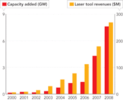
Despite capacity being slashed, there’s no cause for gloom; it’s just that growth rates won’t be at (unsustainable) 40–50% levels for a couple of years. The sector does retain ‘golden’ status for laser tool suppliers owing to: (1) near double-digit growth potential for equipment still forecast for 200910; (2) ‘green’ initiatives (especially North America11) provide stable (long-term) demand; and (3) increasing efficiency8 and lowering fixed/variable manufacturing costs remain top priority. The final point best highlights the opportunity now for laser tooling—as equipment that is ‘enabling’ rather than merely a ‘green’ tooling option or performing a ‘loss-preventative’ task. FIGURE 1 confirms that laser based tool revenues12 (pilot- or full-production) have historically tracked capacity expansions, with growth rates the envy of other industrial laser segments13. (In absolute numbers, a comparison to laser tool revenues within the microelectronics segment14 always puts solar into perspective.)
A mature industry with high utilization rates can forecast tooling based upon production output; however, laser tool supply to solar remains dependent on ‘capacity-build,’ regardless whether product generating or not. Therefore, Figure 1 has strong contributions from pilot-builds within the revenues, more pronounced currently for thin-film. Accurate laser tool forecasting therefore requires knowledge of projected capacity levels across all c-Si and thin-film technologies.
Historic technology drivers
From the early 1980s to the late 1990s, almost all signs for laser tooling within c-Si pointed towards BP-Solar15; as one of the first users of lasers for edge isolation16, and as the undisputed champion of high-efficiency cells with the first laser assisted selective emitter—the LGBC cell17. Early laser adoption was possible due to research at the University of New South Wales18, Sandia Labs19, and EU funded projects ‘LowThermCells’ and ‘LightPrintCells’20. This research discussed almost every use of lasers for high-efficiency production. Since 2000, laser research for c-Si processes has been pioneered throughout Europe including Fraunhofer-ISE21 and LZH/ISFH22.
Thin-film laser-based tooling had a smoother introduction23, with lasers the de facto equipment type for thin-film patterning. When thin-film production went primetime, laser-based tools were consumed at a rate dictated by: (1) capacity expansion plans from the likes of First Solar, Kaneka, and Unisolar (see Ref. 5); (2) the rise of turnkey fab suppliers promoting FPD-style lines7; and (3) R&D and pilot-line CapEx releases from VC-funded start-ups or established c-Si players hedging their bets with thin-film play. Consequently, thin-film laser based tools’ functionality became somewhat ‘prescriptive,’ as opposed to next-generation, technology enabling.
Efficiency & throughput change equipment
The slowdown in capacity expansion coupled with the drive to increase utilization rates, conversion efficiencies, and line throughputs is placing new demands on laser-tools.
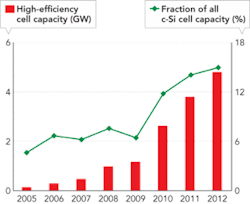
Aside from BP-Solar’s LGBC cells, laser tools have been implemented mainly for edge isolation within c-Si production24. More loss preventative than efficiency enhancing, this nonetheless gave laser tools their entry ticket within the supply chain, and a significant number of lasers25 are run 24/7 here. Production lines have relied mostly upon tried-and-tested process flows to manufacture 13–16% efficient cells; well below the 20%+ from high-efficiency concepts. Reaching high-efficiency status (>17%8) requires different cell architectures, new process steps, and—crucially—new production equipment. And while there are different routes to high efficiency (back-contact, back-junction, selective-emitter, electroless plating, improved passivation), a common theme includes laser based equipment9, 17, 26. FIGURE 2 shows the anticipated growth of high-efficiency cells based on data from Ref. 8.
Laser tools for thin-film have recently become as fragmented as thin-film technology itself; situation which doesn’t help would-be entrants to the supply chain. Differences in absorber materials, TCO layers, panel thicknesses, panel sizes, substrate materials, and throughput levels add to this confusion. And then risk gets factored in. Is there going to be a worthwhile equipment demand for each of a:Si, ‘micromorph’, CdTe, and CIGS variants? Also, there is another differentiating factor between thin-film and c-Si—the role of the turnkey suppliers.
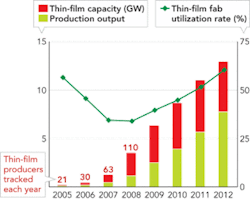
So, a glance at laser tools for thin-film reveals a diverse range of equipment types, each serving some kind of niche. Similar to c-Si, laser based equipment is going through a transition, but not one driven (yet) by technology shakeout. Rather, changes are a direct consequence of the over capacity and CapEx released by the thin-film industry from 2005–2007; there were more than 100 thin-film panel producers counted during 2008. Utilization rates for thin-film lines reached an all-time low by the end of 2008, with overall industry numbers in the low-thirty-percents (see FIGURE 3). Forecasting laser tooling for thin-film is therefore subject to many wildcards, and it’s too early to predict how this will unfold. A safer bet is to focus on existing process stages (glass cutting or border deletion), which are standard across all thin-film variants and have traditionally been served by non-laser-based tools. Here, existing capacity provides a serviceable market, shielded from CapEx decisions. Figure 3 confirms it may be some time before utilization rates top the 90% level, when more structured growth in thin-film may be seen27.
Conclusions
Considerable opportunities still exist for laser based tooling within the solar industry despite the events of the past 12 months. Now though, return-on-investment is being scrutinized more with less credit available for capacity expansion. For c-Si production, this may herald new laser based production equipment, dedicated to high-efficiency cells. In thin-film the short-term outlook is bleaker for the equipment supply chain, requiring a more cautious approach from laser based tool suppliers and possibly fortuitous alignment with eventual winners of any pending thin-film shakeout.
References
- http://www.solid-state.com/display_article/351285/5/none/none/APPLI/The-global-economy-fell-down-and-went-boom----will-solar-follow
- http://www.pv-tech.org/news/_a/major_market_decline_forecasted_for_the_solar_industry_in_2009_according_to/?utm_source=Feeds&utm_campaign=News+Feed&utm_medium=rss
- http://www.pv-tech.org/news/_a/suntech_halts_capacity_expansion_slashes_capital_spending_for_2009/
- W. Hirshman, “Little smiles on long faces,” Photon International, 3, 2009.
- http://www.pv-tech.org/news/_a/isuppli_reveals_the_winners_and_loser_in_the_solar_industry_shakeout/?utm_source=Feeds&utm_campaign=News+Feed&utm_medium=rss
- /content/ils/en/display_article/357522/39/none/none/IndUp/Industrial-Laser-Solutions-revises-laser-industry-forecast
- http://www.pvworld.com/pvworld/en-us/index/articles/display.articles.Photovoltaics-World.equipment-and_materials.manufacturing-equipment.turnkey-manufacturing.QP129867.dcmp=rss.page=1
- N. Mason, “High efficiency crystalline silicon PV cell manufacture: status and prospects,” PVSAT-5, Glyndw^r, 2009.
- F. Colville, “Laser processing enables high-efficiency silicon-cell concepts,” Photovoltaics World, 1, p.44, March 2009.
- http://www.semiconductor.net/article/CA6638576.html
- http://www.pv-tech.org/news/_a/president_obama_signs_stimulus_bill_solar_trade_groups_applaud/?utm_source=Feeds&utm_campaign=News+Feed&utm_medium=rss
- F. Colville, ‘The market for laser-based processing of solar cells’, at Lasers & Photonics Marketplace Seminar, San Jose, January 2009.
- D. Belforte, ‘World markets for industrial lasers and applications’, at Lasers & Photonics Marketplace Seminar, San Jose, January 2009.
- http://www.semiconductor.net/article/CA6628545.html?nid=3663
- F. Colville, “Into the groove; how buried contacts brought lasers to life in solar,” InterPV, June 2009.
- N. Mason, private communication, April 2009.
- F. Colville, “Laser assisted selective emitters & the role of laser doping,” Photovoltaics International, 5, 2009.
- M. Green, Silicon solar cells: Advanced principles and practice, Center for Photovoltaic Devices and Systems, Sydney, Australia, 1995.
- D. King et al., “Development of a multi-purpose, pulsed-laser system for solar cell processing applications,” 21st IEEE PVSC, Orlando, 1990.
- L. Pirozzi et al., “Innovative applications of laser technology in photovoltaics,” Proc. SPIE Conf. on Laser Applications in Microelectronic & Optoelectronic manufacturing II, San Jose, 1997.
- A. Gröhe et al., “Laser processes for the industrial production of high efficiency silicon solar cells,” 22nd EUPVSEC, Milan, 2007.
- P. Engelhart et al., “Laser processing for back-contacted silicon solar cells,” ICALEO LMC, Paper M703, Scottsdale, 2006.
- A. Compaan et al., “Laser scribing of polycrystalline thin films,” Optics and Lasers in Engineering, 34, 2000.
- F. Colville, “Lasers edge in front,” Global Solar Technology, March/April, 2009.
- /content/ils/en/display_article/360165/39/none/none/IndUp/Coherent-ships-100th-AVIA-laser-for-solar-cell-production
- F. Colville, et al., ‘Existing and emerging laser applications within PV manufacturing’, Photovoltaics International, 1, 2008.
- http://www.euroasiasemiconductor.com/solar_news_full.php?id=10685
About the Author
Finlay Colville
Dr. Finlay Colville has been Head of Research at PV-Tech and Solar Media Ltd since 2015. Before this, he spent 5 years as VP and head of solar at market research firm NPD Solarbuzz, and 10 years in various sales and marketing roles at Coherent, Inc. Dr. Colville holds a BSc in Physics from the University of Glasgow and a PhD in nonlinear photonics from the University of St. Andrews.


