Nanosecond pulsed fiber lasers—more than just markers
This decade has seen the rapid adoption of fiber laser technology as a prime contender for materials processing applications at the 1 micron wavelength, especially for marking where they represent one in three laser sources. Fiber laser sources offer users a compact, low-cost solution that has no maintenance requirements and therefore yields a low cost of ownership solution. For non-technical users it is a fit-and-forget option.
Maintaining beam quality is often a challenge for many laser types due to degradation of optics, thermal lensing, or other alignment effects experienced with gas or rod-based lasers. In fact, specific modes can be optically engineered to meet specific materials processing applications.
The latest generation of nanosecond pulsed fiber lasers are compact, highly flexible sources with tailored beam quality and a range of configurable pulse options. These give a further dimension for process enhancement in most applications. Recent increases in peak powers and pulse energies are opening new applications beyond conventional marking, making these lasers into highly capable micromachining tools.
Many fiber lasers are based on a Q-switch type design and mimic the capabilities of other solid-state lasers. These sources, still the workhorses for current marking applications, are limited in their ability to optimize pulse parameters limiting repetition rates to <100 kHz. Fiber lasers with sophisticated Master Oscillator Power Amplifier (MOPA) designs, using directly modulated seed lasers and amplifier chains, allow flexibility in the control of pulse parameters such as pulse length and frequency.
For example, SPI’s latest MOPA design enables high peak powers that are not achieved with standard modulation, with some models producing peak pulse powers in excess of 20 kW and >1.25 mJ pulse energies at 30 kHz giving an average output power of 40W. These units also have a high pulsing frequency range from 1 to 500 kHz and with variable pulse widths in the 10–200 ns range as well as having the capability of working in continuous wave (CW) mode.
In materials processing there are a number of key parameters that can affect quality and productivity and these include peak pulse power (kW), pulse energy (mJ), pulse frequency (kHz), average power (W), pulse duration (ns), and beam quality (M2). A combination of all of these parameters needs to be considered in the majority of pulsed laser materials processing applications.
The nature of pulsed processing relies heavily on overlapping laser spots to achieve the desired result. It is widely accepted that >30% spot-to-spot overlap is the sweet spot for many laser processes although at higher overlaps the resultant mark appearance is almost continuous. The ability to go to high repetition rates means that higher processing speeds can be achieved. At 500 kHz, this 30% spot overlap can be achieved at scanning speeds as high as 8 m/s.
Sensitive materials that require careful control of heat input can often be processed better with shorter pulses and higher repetition rates. Processing plastic and polymeric materials particularly benefit from the ability to maintain the peak power and limit the overall heat input per unit length (see FIGURE 1). Other applications specifically benefiting from >100 kHz operation include paint removal (night and day marks), color marking, IC marking and thin film patterning (solar cell and LCD screen).
Beam quality has a critical effect on many applications and should be taken in the context of fitness for purpose as it is not always the case that a low M2 is better. Low M2 beams give smaller spots with a greater depth of processing field, but the higher peak power can lead to excessive center point intensity leading to problems such as substrate damage in thin film patterning or cleaning type processing applications. The smaller spot also requires more passes when covering larger areas due to smaller line spacing. For such applications higher M2 are preferable giving a broader power distribution more suited to area processing.
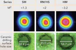
At SPI we have developed a range of pulsed lasers that covers a broad range of applications with nominally different beam quality requirements (see FIGURE 2). The impact of the beam quality of the lasers is quite dramatic and is predominantly linked to the focused spot sizes that can be achieved. Comparative studies show the impact of the spot size on marking and drilling applications. The single mode pulsed laser generates a narrow and deep high-aspect-ratio hole while the higher mode lasers generate progressively wider and shallower holes given the same number of laser pulses. This result is perhaps obvious to many but it should be noted that the final features do not necessarily correspond strictly to the calculated spot size. The choice depends on the requirements of the application.Soldering is typically regarded as a direct diode or CW fiber laser process, however, for thermally sensitive applications the conventional laser based techniques can not control the heat input sufficiently. Using a pulsed fiber laser at high rep rate, combined with a rapid scanning technique, reflow soldering can be achieved with lower overall heat input to the part.
The range of applications for nanosecond fiber lasers is currently growing as users are becoming aware of their flexibility and versatility of the newer MOPA designs. The availability of tailored mode qualities and variable pulse characteristics are helping to open up the application space.
Now nanosecond fiber lasers have matured and elevated themselves from just marking lasers to far more capable micromachining tools. So whatever the micromachining applications the potential use of pulsed fiber lasers is worth considering.
About the Author
Jack Gabzdyl
Industry Manager – Electronics, TRUMPF Laser UK Ltd
Dr. Jack Gabzdyl is Industry Manager – Electronics at TRUMPF Laser UK Ltd (Southampton, England) and has more than 30 years of laser materials processing experience. He obtained his PhD in laser processing from Imperial College London in 1989. He has since had a number of technical and marketing positions at BOC Gases, Advanced Laser Solutions, and TWI before joining TRUMPF (formerly SPI Lasers) in 2007.
