Photodetectors: Radiation-hardened InGaAs photodiodes survive rugged space-based qualification testing
Despite the need for radiation-hardened, space-qualified photodetectors for inter- and intra-satellite laser-based communication links, gravitational-wave detection, and in referencing systems for space-based lidar and optical clocks, there are few commercially available photodiodes that meet the harsh conditions of space.
Since 2006, Discovery Semiconductors (Ewing, NJ) has focused on developing radiation-hardened, space-qualified indium gallium arsenide (InGaAs) photodetectors based on an ultrafast dual-depletion region InGaAs photodiode structure that is inherently resilient to radiation.
To date, they have radiation-tested multigigahertz, 1060–1650 nm wavelength lattice-matched InGaAs photodetectors, lattice-mismatched InGaAs photodetectors for extended wavelengths up to 2200 nm, and large-area ultralow-noise quad photoreceivers for gravitational-wave detection. Furthermore, some of these devices have flown on the International Space Station (ISS) as part of MISSE 7 and the ongoing MISSE 9 mission.
The qualification of these uncooled devices sheds light on fabrication methods that can serve not only space-based, but a variety of terrestrial photodiode applications for harsh environments.
DDR revelations
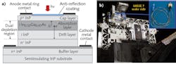
Standard p-i-n InGaAs photodiodes have an intrinsic region with a low-bandgap InGaAs absorption layer (around 0.74 eV). Defined by capacitance and carrier transit time, the bandwidth depends on careful consideration of the optimum absorption layer thickness. To relax this tradeoff, the dual-depletion region (DDR) architecture—designed by Discovery Semiconductors in 1994 and since improved—maximizes bandwidth via a top-illuminated geometry wherein a nonabsorbing indium phosphide (InP) draft layer (1.35 eV) in the intrinsic region is used to balance the transit times of faster photogenerated electrons and slower holes, reducing capacitance without increasing overall transit time and enabling photodiodes with a bandwidth up to 65 GHz. The restricted thickness of the low-bandgap InGaAs depletion region also improves radiation hardening.
Space-readiness testing for the DDR architecture with both broad-wavelength and lattice-matched designs at the Fraunhofer Institute for Technological Trend Analysis (Fraunhofer INT; Euskirchen, Germany) included 35 MeV proton radiation with a total ionizing dose (TID) up to 50 krad and irradiation by 1 MeV gamma rays from a cobalt 60 source up to a 50 krad dose, with no significant change observed in dark current or DC and AC responsivity. In addition, packaged modules survived mechanical shock and vibration tests to verify survivability during space launch.
Some of these modules survived for 18 months on the ISS as part of the MISSE 7 payload and withstood extreme temperatures up to 16 times a day, proton radiation from the inner Van Allen belt at the South Atlantic Anomaly, and galactic cosmic rays. Two photodiode modules are now spaceborne on the European Space Agency (ESA) Aelous mission as part of Tesat Spacecomm’s Laser Reference Head, and two more are scheduled for launch as part of the ESA EarthCARE mission in 2019 (see figure).
In addition, since 2017, both InGaAs photodiodes and GaAs as well as silicon RF amplifiers have been undergoing further comprehensive radiation testing at the NASA Space Radiation Laboratory (NSRL; Brookhaven, NY) to quantify their tolerance to protons, gamma rays, helium, and heavy iron for NASA’s future Earth science as well as outer space missions.
About the Author

Gail Overton
Senior Editor (2004-2020)
Gail has more than 30 years of engineering, marketing, product management, and editorial experience in the photonics and optical communications industry. Before joining the staff at Laser Focus World in 2004, she held many product management and product marketing roles in the fiber-optics industry, most notably at Hughes (El Segundo, CA), GTE Labs (Waltham, MA), Corning (Corning, NY), Photon Kinetics (Beaverton, OR), and Newport Corporation (Irvine, CA). During her marketing career, Gail published articles in WDM Solutions and Sensors magazine and traveled internationally to conduct product and sales training. Gail received her BS degree in physics, with an emphasis in optics, from San Diego State University in San Diego, CA in May 1986.