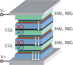
Engineers at Osram AG (Munich, Germany) have developed a stacked organic light-emitting diode (OLED) architecture that improves output characteristics and increases lifetime compared to conventional single-active-layer OLEDs. In the stacked-OLED process, undoped and organic active layers—the emissive layer (EML) with red/green/blue (RGB) layers—are first embedded in p-type and n-type doped layers to create a single p-i-n diode or single-active-layer OLED. When three devices are stacked, for example, electron-hole pairs are created at charge-generation layers (CGLs). A twofold white-emitting stacked device achieves the same luminance levels as a single p-i-n device at half the current and twice the voltage.
Because stacked devices have a much higher differential resistivity, stacking improves uniformity of large-area OLEDs without the need to deposit thin metal bus lines on the transparent conductive oxide layer. And because the individual emission values (and corresponding aging mechanisms such as temperature and current density) are lowered for each layer in a stacked device, the overall stacked OLED has a longer lifetime. Contact Christian Boelling at [email protected].
About the Author

Gail Overton
Senior Editor (2004-2020)
Gail has more than 30 years of engineering, marketing, product management, and editorial experience in the photonics and optical communications industry. Before joining the staff at Laser Focus World in 2004, she held many product management and product marketing roles in the fiber-optics industry, most notably at Hughes (El Segundo, CA), GTE Labs (Waltham, MA), Corning (Corning, NY), Photon Kinetics (Beaverton, OR), and Newport Corporation (Irvine, CA). During her marketing career, Gail published articles in WDM Solutions and Sensors magazine and traveled internationally to conduct product and sales training. Gail received her BS degree in physics, with an emphasis in optics, from San Diego State University in San Diego, CA in May 1986.