First LEDs fabricated on amorphous glass substrates
Researchers at the Samsung Advanced Institute of Technology (Yongin, South Korea) and Seoul National University (Seoul, Korea) have demonstrated the first LEDs to be fabricated on amorphous glass substrates. Because gallium nitride (GaN)-based LEDs grown on crystalline sapphire wafers are expensive and not amenable to large-sized wafer arrays, GaN LEDs on silicon substrates (GaN-on-Si) are an improved alternative. However, GaN LEDs on amorphous glass substrates offer even lower manufacturing costs, easier scalability to large-sized LED arrays, and potential use as emissive devices due to the transparency of the glass substrate material.
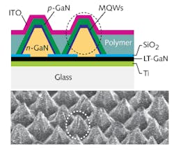
The secret to controlled growth of the five-period indium GaN/GaN (InGaN/GaN) multiple quantum wells that comprise the emissive layer in the pyramidal-shaped LED array is a thin-film titanium pre-orienting layer that is similar to the GaN hexagonal crystal structure. Following the pre-orienting layer and the initial low-temperature GaN layer (LT-GaN) is a hole-patterned silicon dioxide (SiO2) layer that further defines the nucleation sites for the emissive-layer growth stages using a local heteroepitaxy process. After polymerization of the pyramidal structures and a final indium tin oxide (ITO) electrode layer, the pyramidal LED devices were found to emit illumination in the range from 448–478 nm with an approximate luminance of 600 cd/m2. Contact Jong Min Kim at [email protected].
About the Author

Gail Overton
Senior Editor (2004-2020)
Gail has more than 30 years of engineering, marketing, product management, and editorial experience in the photonics and optical communications industry. Before joining the staff at Laser Focus World in 2004, she held many product management and product marketing roles in the fiber-optics industry, most notably at Hughes (El Segundo, CA), GTE Labs (Waltham, MA), Corning (Corning, NY), Photon Kinetics (Beaverton, OR), and Newport Corporation (Irvine, CA). During her marketing career, Gail published articles in WDM Solutions and Sensors magazine and traveled internationally to conduct product and sales training. Gail received her BS degree in physics, with an emphasis in optics, from San Diego State University in San Diego, CA in May 1986.