Waveguide mode converters have wide bandwidth, small footprint
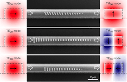
Columbia University (New York, NY) researchers have invented a method to control the modes light propagating in waveguides with high efficiency by using nanoantennas.1 To demonstrate this technique, they built photonic integrated devices that not only had record-small footprints but were also able to maintain optimal performance over an unprecedented broad wavelength range.
The data rate for waveguides in photonic integrated circuits can be boosted by channeling date via a multiple number of modes rather than just a single mode, a technique called mode-division multiplexing (MDM); however, the ability to manipulate modes then becomes very important. That's where mode converters come in.
The optical power of light waves propagating along waveguides is confined within the core of the waveguide: researchers can only access the guided waves via the small evanescent "tails" that exist near the waveguide surface. These guided waves are particularly hard to manipulate and so photonic integrated devices are often large in size, taking up space and thus limiting the device integration density of a chip.
The Columbia team found that the most efficient way to control light in waveguides is to "decorate" the waveguides with optical nanoantennas, which pull light from inside the waveguide core, modify the light’s properties, and release light back into the waveguides. The accumulative effect of a densely packed array of nanoantennas is so strong that they could achieve functions such as waveguide mode conversion within a propagation distance no more than twice the wavelength.
"This is a breakthrough considering that conventional approaches to realize waveguide mode conversion require devices with a length that is tens of hundreds of times the wavelength," says Nanfang Yu, a professor at Columbia and one of the researchers. "We've been able to reduce the size of the device by a factor of 10 to 100."
Yu plans next to incorporate actively tunable optical materials into the photonic integrated devices to enable active control of light propagating in waveguides. Such active devices will be the basic building blocks of augmented-reality goggles that first determine the eye aberrations of the wearer and then project aberration-corrected images into the eyes, which he and his Columbia Engineering colleagues, Michal Lipson, Alex Gaeta, Demetri Basov, Jim Hone, and Harish Krishnaswamy are working on now. Yu is also exploring converting waves propagating in waveguides into strong surface waves, which could eventually be used for on-chip chemical and biological sensing.
Source: http://engineering.columbia.edu/news/nanfang-yu-light-propagation-waveguides
REFERENCE:
1. Zhaoyi Li et al., Nature Nanotechnology (2017); doi: 10.1038/nnano.2017.50
About the Author

John Wallace
Senior Technical Editor (1998-2022)
John Wallace was with Laser Focus World for nearly 25 years, retiring in late June 2022. He obtained a bachelor's degree in mechanical engineering and physics at Rutgers University and a master's in optical engineering at the University of Rochester. Before becoming an editor, John worked as an engineer at RCA, Exxon, Eastman Kodak, and GCA Corporation.