Fraunhofer HHI and partners develop market-ready polymer optical chips
A European project called the PolyPhotonics Innovation Initiative is developing polymer-based integrated optics for the global communications market. Part of the Regional Enterprise Initiative of the German Federal Ministry of Research, the project will build the value chain that will make this new technology platform practical. The Fraunhofer Heinrich Hertz Institute (HHI; Berlin, Germany) is coordinating the project.
Eleven regional enterprises and three research institutes are pooling their expertise in PolyPhotonics Berlin. The network partners aim to implement comprehensive solutions using optical components made of plastic, which are globally not yet available in this form. The participants in this initiative want to create innovative materials and procedures for the production and assembly of photonic multiple-use components.
The PolyPhotonics technology platform provides a toolbox of hybrid-optical building blocks. Using suitable technologies, members of the initiative put these basic building blocks together to form flexible modules for integration into compact functional components of very flexible build (hybrid integration).
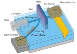
At the core of the platform is a chip with polymer optical waveguides. The chip may feature further passive elements such as optical fibers, thin-film filters, and micro-optics as well as active elements such as photodiodes or laser chips. These components are tested in the group's laboratories and will be further developed to the point where they are market-ready.
The unique aspect is the use of polymer as material for waveguide boards. In one example, a board is needed as a component for a future socket outlet (see figure). This outlet must be ready when data arrives via fiber-optic cable. The miniature 1 x 5 mm polymer chips in those sockets can be used in applications other than plug-in connectors as well.
Source: Fraunhofer Heinrich Hertz Institute
About the Author

John Wallace
Senior Technical Editor (1998-2022)
John Wallace was with Laser Focus World for nearly 25 years, retiring in late June 2022. He obtained a bachelor's degree in mechanical engineering and physics at Rutgers University and a master's in optical engineering at the University of Rochester. Before becoming an editor, John worked as an engineer at RCA, Exxon, Eastman Kodak, and GCA Corporation.