Fujitsu and partners halve power requirements for silicon photonic transceivers
Fujitsu Limited (Tokyo, Japan), Fujitsu Laboratories of America (Sunnyvale, CA), the Photonics Electronics Technology Research Association (PETRA; Japan), and the New Energy and Industrial Technology Development Organization (NEDO; Kawasaki, Japan) have jointly developed the world's most energy efficient silicon photonics optical transceiver circuit for high-speed data transmissions between CPUs in servers and supercomputers, requiring only 5 mW of electricity per 1 Gbps of transmission speed.
Related Article
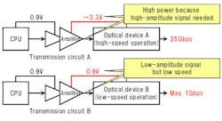
Optical devices have needed a certain amount of voltage in order to run at high speeds, making it difficult to reduce the power needed for optical transceiver circuits. Now Fujitsu and its partners have developed a technology that allows optical devices to be run at a low voltage by significantly increasing amplitude when there is a change in the data being transmitted, resulting in high-speed operations of 25 Gbps at half the power previously required.
While reducing the amount of power consumed, this technology enables multiple optical transceiver circuits to run in parallel for high-speed, terabit-class transmissions, and is therefore expected to raise the performance of servers and supercomputers.
Parts of this technology were developed in the "Integrated Photonics-Electronics Convergence System Technology (PECST)" project that NEDO entrusted to PETRA, while Fujitsu Limited, Fujitsu Laboratories, and Fujitsu Laboratories of America are collaborating to develop the transceiver circuit technology.
Improving the performance of servers and requires not just raising the calculating performance of each individual CPU, but also raising the speed of data transmissions between connected CPUs. Overall systems for servers and supercomputers require significant amounts of power, but due to constraints on the amount of power facilities can supply, there is a desire to increase the data transmission speeds of transceiver circuits without increasing the amount of power consumed.
For silicon photonics-based optical transceiver technology, which holds significant promise for the next generation of high-performance supercomputers, optical devices are effectively limited to transmission speeds of 25 Gbps. One way of increasing overall transmission speeds is to run in parallel multiple optical devices and the electronic circuitry of their optical transceiver circuits. There is a need to double the speed of data transmissions between CPUs in four years. So to achieve this doubling while holding power constant, the power consumed by optical transceiver circuits needs to be cut in half.
By amplifying the transmission signal only when the signal from the CPU changes to -1 and +1, the researchers on this project succeeded at generating amplitudes intermittently at around 1.8 V. As a result, the supplied voltage is 1.8 V, lower than the 3.3 V previously required, and because power is not used with smaller amplitudes when the data do not change, less power is consumed. The principal behind this technology is that the data being transmitted is combined with delayed data that is multiplied by -α (where 0 < α < 1), so that when the transmission data changes from -1 to +1, +1 is amplified to +1+α. On the other hand, when the transmission data changes from +1 to -1, -1 can be amplified further to -1-α.
This technology enables both higher speeds and lower power consumption, and the researchers on the project confirmed that they could achieve high-speed transmissions of 25 Gbps while operating at half the power previously required, achieving operation of 5 mW of electricity per 1 Gbps of transmission speed.
SOURCE: Fujitsu; http://www.fujitsu.com/global/about/resources/news/press-releases/2015/0223-02.html
About the Author

Gail Overton
Senior Editor (2004-2020)
Gail has more than 30 years of engineering, marketing, product management, and editorial experience in the photonics and optical communications industry. Before joining the staff at Laser Focus World in 2004, she held many product management and product marketing roles in the fiber-optics industry, most notably at Hughes (El Segundo, CA), GTE Labs (Waltham, MA), Corning (Corning, NY), Photon Kinetics (Beaverton, OR), and Newport Corporation (Irvine, CA). During her marketing career, Gail published articles in WDM Solutions and Sensors magazine and traveled internationally to conduct product and sales training. Gail received her BS degree in physics, with an emphasis in optics, from San Diego State University in San Diego, CA in May 1986.

